Layout method of semiconductor device and method of forming semiconductor device

a semiconductor device and layout method technology, applied in the direction of cad circuit design, computer aided design, instruments, etc., can solve the problems of increasing complications, increasing the difficulty of layout and then fabricating contacts and interconnections, and reducing the width of interconnections and distances between

Inactive Publication Date: 2016-02-11
SAMSUNG ELECTRONICS CO LTD
View PDF0 Cites 2 Cited by
  • Summary
  • Abstract
  • Description
  • Claims
  • Application Information

AI Technical Summary

Problems solved by technology

As semiconductor devices become more highly integrated, the widths of interconnections and distances therebetween are being reduced leading to increasing complications.
That is, it is becoming increasingly difficult to layout and then fabricate contacts and interconnections electrically connected to the contacts when manufacturing semiconductor devices according to design rules in demand.

Method used


Image

  • Layout method of semiconductor device and method of forming semiconductor device
  • Layout method of semiconductor device and method of forming semiconductor device
  • Layout method of semiconductor device and method of forming semiconductor device

Examples


Embodiment Construction

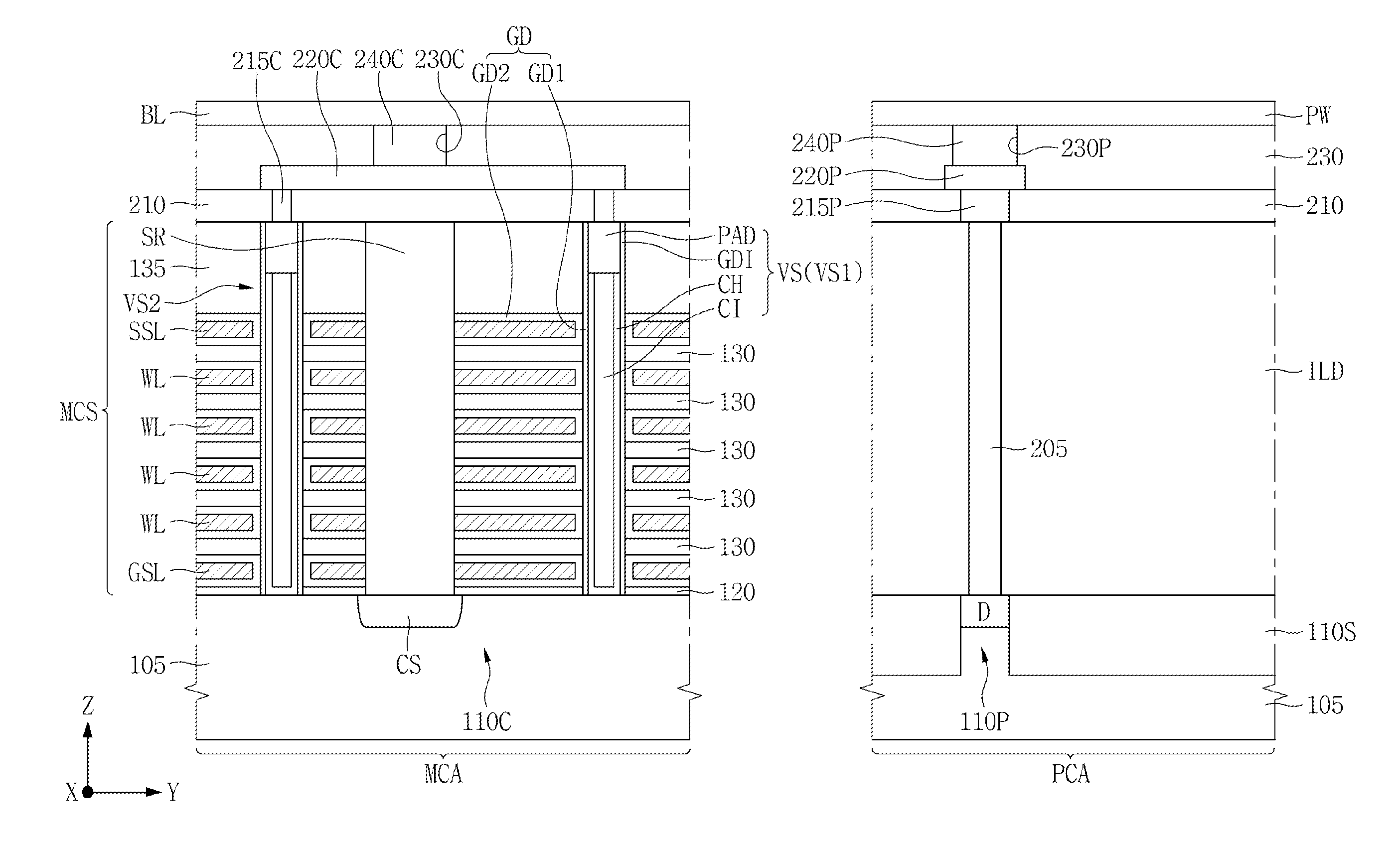
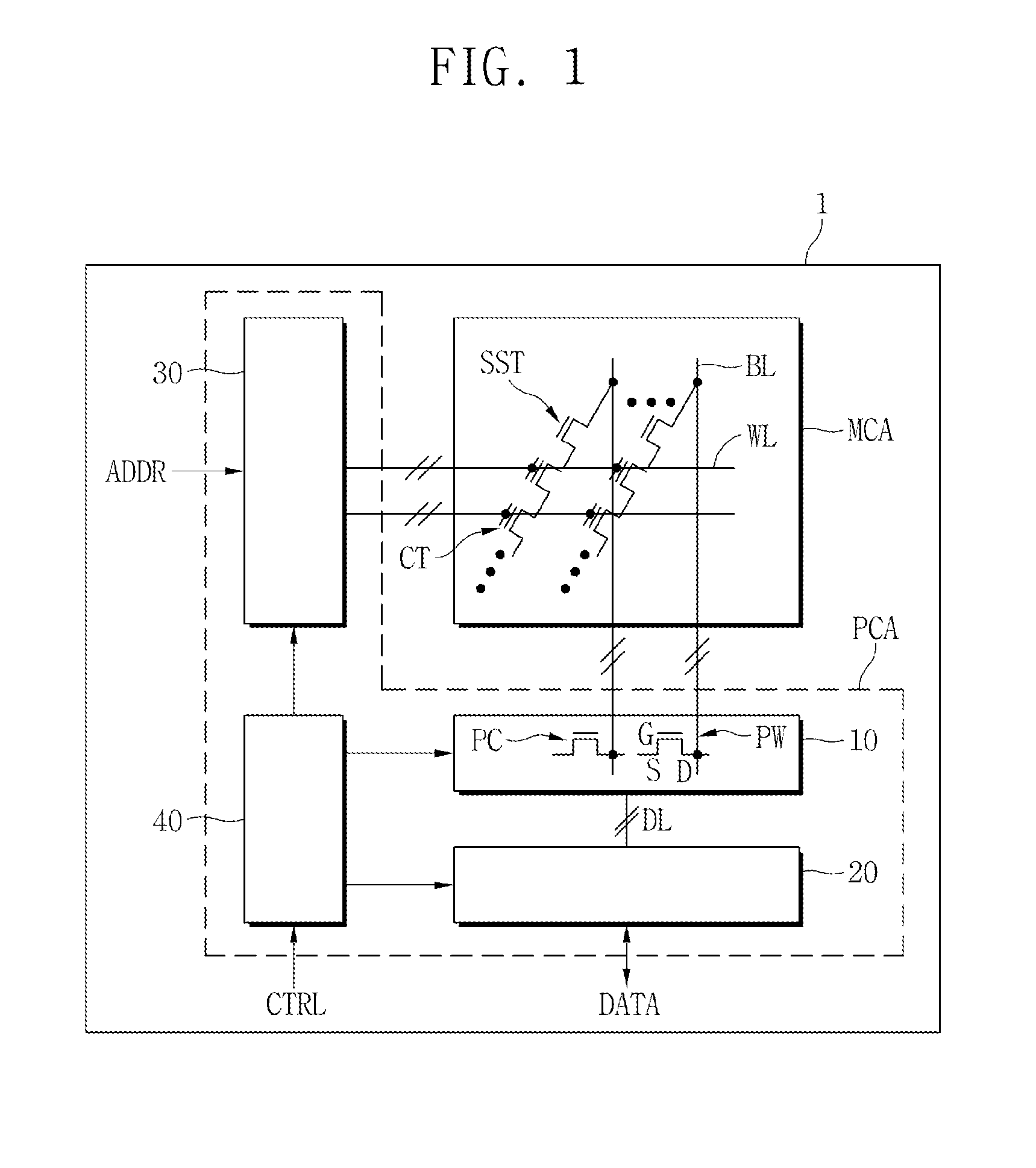
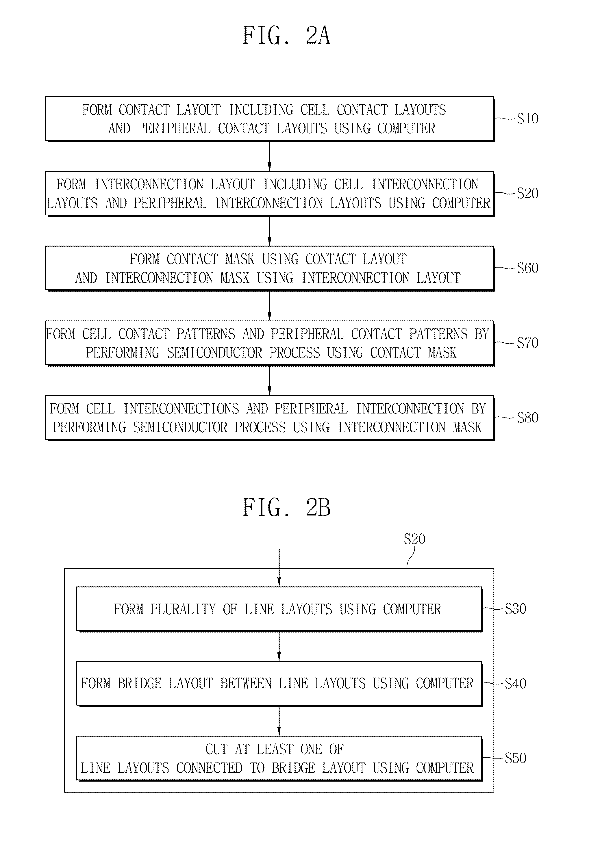
[0021]Various embodiments will now be described more fully with reference to the accompanying drawings in which some embodiments are shown. These inventive concepts may, however, be embodied in different forms and should not be construed as limited to the embodiments set forth herein. Rather, these embodiments are provided so that this disclosure is thorough and complete and fully conveys the inventive concept to those skilled in the art. In the drawings, the sizes and relative sizes of layers and regions may be exaggerated for clarity. Like numerals refer to like elements throughout.

[0022]The exemplary embodiments of the invention will be described with reference to cross-sectional views, plan views, and block diagrams, which are ideal exemplary views. Forms of the embodiments may be modified by the manufacturing technology and / or tolerance. Therefore, the embodiments of the invention are not intended to be limited to illustrated specific forms, and include modifications of forms g...


PUM


Abstract

A layout method for use in fabricating a semiconductor device includes creating a contact layout including cell contact layouts and peripheral contact layouts using a computer, and creating an interconnection layout including cell interconnection layouts and peripheral interconnection layouts using the computer. The interconnection layout includes a plurality of line layouts and bride layouts. The line layouts include cell interconnection layouts and peripheral line layouts. The peripheral line layouts include a first peripheral line layout and a second peripheral line layout adjacent to each other, and the peripheral contact layouts include a misaligned contact layout interposed between the first and second peripheral line layouts. The bridge layout connects the first and second peripheral line layouts and overlaps the misaligned contact layout. In the method, the second peripheral line layout is divided along its length.

Description

PRIORITY STATEMENT[0001]This application claims priority under 35 U.S.C. §119 to Korean Patent Application No. 10-2014-0100577 filed on Aug. 5, 2014, the disclosure of which is hereby incorporated by reference in its entirety.BACKGROUND[0002]1. Technical Field[0003]Embodiments of the inventive concept relate to a layout method of a semiconductor device and to a method of manufacturing the semiconductor device using the same.[0004]2. Description of Related Art[0005]As semiconductor devices become more highly integrated, the widths of interconnections and distances therebetween are being reduced leading to increasing complications. Thus, the random locations available for contacts of the devices are gradually becoming reduced. That is, it is becoming increasingly difficult to layout and then fabricate contacts and interconnections electrically connected to the contacts when manufacturing semiconductor devices according to design rules in demand.SUMMARY[0006]In accordance with an aspec...

Claims


Application Information

Patent Timeline
Patent Type & Authority Applications(United States)
IPC IPC(8): H01L21/311G06F17/50H01L21/768H01L23/528
CPCG06F17/5077G06F17/5072H01L23/528H01L21/76877H01L21/31144H01L21/76802G06F30/394G06F30/392G06F30/39H10B43/10H10B43/40H10B43/27
Inventor CHANG, JI-YOON
Owner SAMSUNG ELECTRONICS CO LTD
Why Eureka
Try Eureka