Optical modulation device including a liquid crystal and an optical display device using the same

a technology of optical modulation and liquid crystal, applied in optics, instruments, electrical devices, etc., can solve the problems of complicated display driving and the inability to obtain the desired light deflection angle, and achieve the effect of simplifying the driving schem

Active Publication Date: 2016-07-14
SAMSUNG DISPLAY CO LTD
View PDF0 Cites 4 Cited by
  • Summary
  • Abstract
  • Description
  • Claims
  • Application Information

AI Technical Summary

Benefits of technology

[0008]According to an exemplary embodiment of the present invention, an optical modulation device may adjust an in-plane rotation angle of liquid crystal molecules to modulate a phase of light and simplify a driving scheme.
[0009]According to an exemplary embodiment of the present invention, a manufacturing process of an optical modulation device including liquid crystals may be simplified and the diffraction efficiency of the optical modulation device may be increased.
[0010]According to an exemplary embodiment of the present invention, a display device that uses an optical modulation device including liquid crystals may have a simplified manufacturing process.

Problems solved by technology

This, however, may complicate display driving.
Further, a desired light deflection angle may not be obtained due to minute electrode patterns used in the manufacturing of the display device.

Method used


Image

  • Optical modulation device including a liquid crystal and an optical display device using the same
  • Optical modulation device including a liquid crystal and an optical display device using the same
  • Optical modulation device including a liquid crystal and an optical display device using the same

Examples


Embodiment Construction

[0047]The present invention will be described more fully hereinafter with reference to the accompanying drawings, in which exemplary embodiments of the present invention are shown. Those skilled in the art would realize that the described embodiments may be modified in various different ways.

[0048]In the drawings, the thicknesses of layers, films, panels, regions, or the like, may be exaggerated for clarity. Like reference numerals may correspond to like elements throughout the specification. It will be understood that when an element such as a layer, film, region, or substrate is referred to as being “on” another element, it may be directly on the other element or intervening elements may be present.

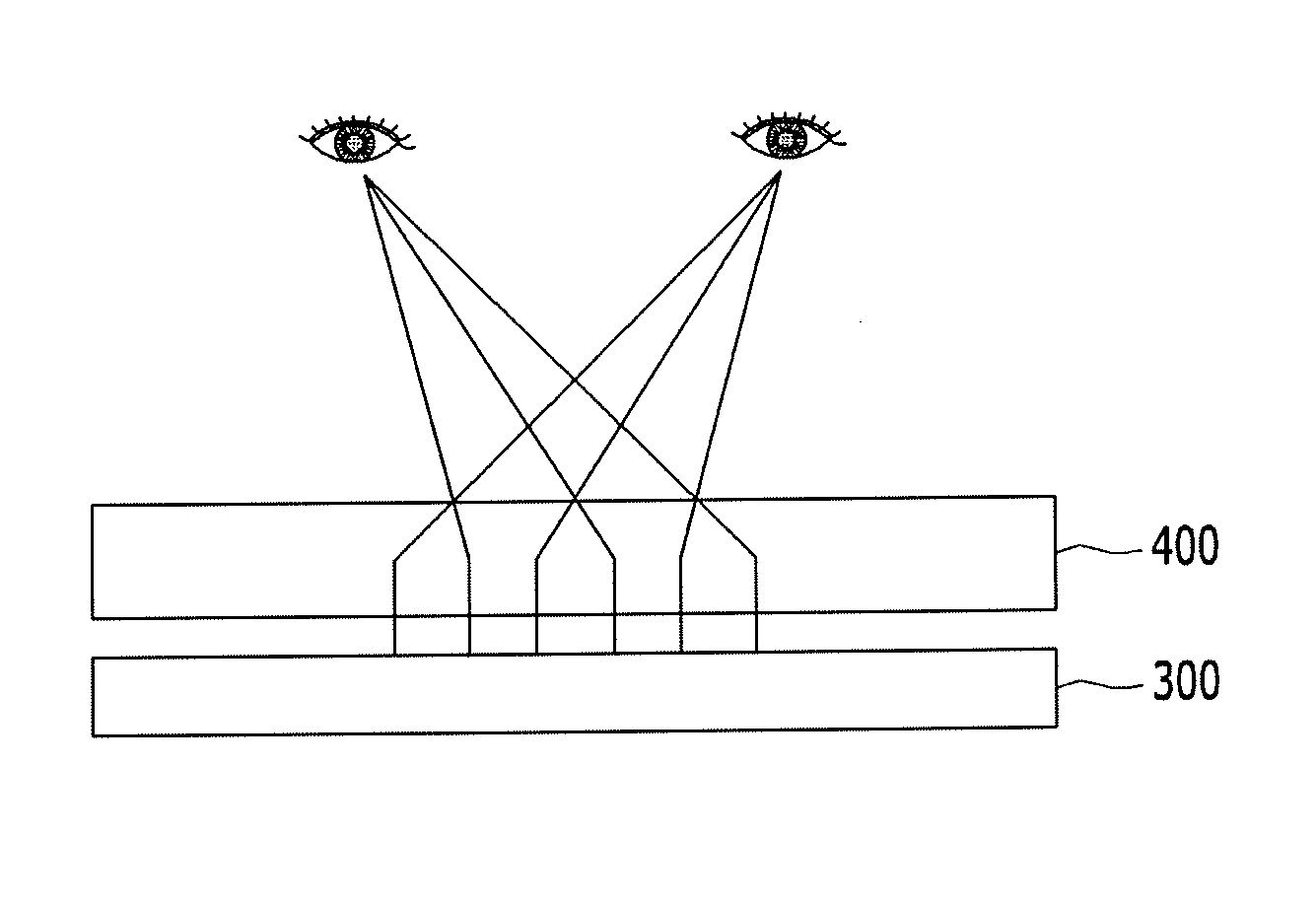
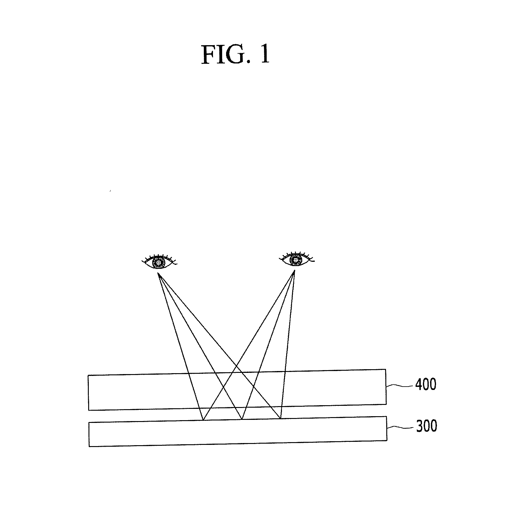
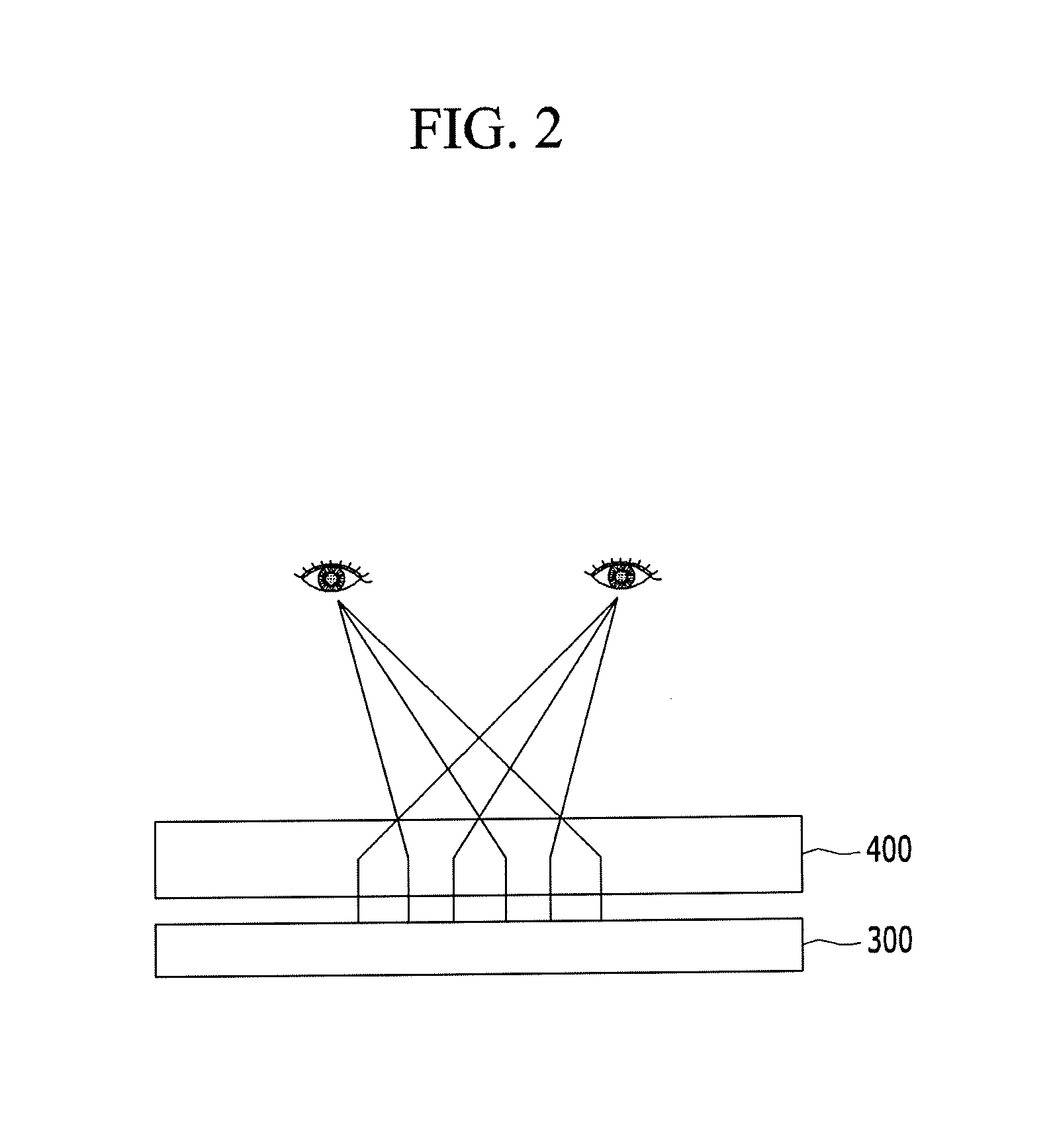
[0049]FIG. 1 is a drawing illustrating an optical display device and a method of generating a two-dimensional (2D) image, according to an exemplary embodiment of the present invention. FIG. 2 is a drawing illustrating an optical display device and a method of generating a three-dimensio...


PUM

PropertyMeasurementUnit
light deflection angleaaaaaaaaaa
non-conductiveaaaaaaaaaa
electric fieldaaaaaaaaaa

Abstract

An optical modulation device, according to an exemplary embodiment of the present invention, includes first and second plates facing each other, the first and second plates including a plurality of regions, and a liquid crystal layer interposed between the first and second plates, the liquid crystal layer including liquid crystal molecules aligned in a vertical alignment (VA) mode. The first plate includes a non-conductive layer including stepped structures repeatedly arranged in a first direction, a first electrode formed to partially cover the non-conductive layer, and first and second aligners disposed in a second direction different from the first direction, wherein the first and second aligners are aligned in opposite directions with respect to each other. The second plate includes a second electrode.

Description

CROSS-REFERENCE TO RELATED APPLICATION(S)[0001]This application claims priority under 35 U.S.C. §119 to Korean Patent Application No. 10-2015-0004337, filed on Jan. 12, 2015, in the Korean Intellectual Property Office, the disclosure of which is incorporated by reference herein in its entirety.TECHNICAL FIELD[0002]Exemplary embodiments of the present invention relate to an optical modulation device and an optical display device using the same, and more particularly, to an optical modulation device including liquid crystals and an optical display device using the same.DISCUSSION OF THE RELATED ART[0003]Optical display devices may use optical modulation devices for modulating characteristics of light. For example, in an optical display device for displaying a three-dimensional (3D) image, an optical modulation device may be used to divide an image with different viewpoints to be transmitted so that a viewer can perceive the image as a stereoscopic image. Optical modulation devices tha...

Claims


Application Information

Patent Timeline
Patent Type & Authority Applications(United States)
IPC IPC(8): G02B27/22G02F1/1337G02F1/1343G02F1/29G02B30/28G02B30/29
CPCG02F1/1337G02F1/13439G02F1/29G02B27/225G02F1/134309G02F1/133776G02F1/294G02B30/28G02B30/29H04N13/30G02B26/06G02B30/34G02B30/27
Inventor JUNG, KYUNG HOSEO, HYUN SEUNGCHOI, CHUN KI
Owner SAMSUNG DISPLAY CO LTD
Why Eureka
Try Eureka