

Multi-Layer, Multi-Material Micro-Scale and Millimeter-Scale Devices with Enhanced Electrical and/or Mechanical Properties
a multi-material, micro-scale and millimeter-scale technology, applied in the direction of instruments, chemistry apparatus and processes, transportation and packaging, etc., can solve the problem of destructive separation of masking material from substra
- Summary
- Abstract
- Description
- Claims
- Application Information
AI Technical Summary
Benefits of technology
Problems solved by technology
Method used
Image

Examples
first embodiment
[0113]The first embodiment provides a method for forming a multi-layer structure using a shell structural material, a core structural material and at least one sacrificial material with only a single selective patterning needing to occur per layer and wherein under general circumstances only partial encapsulation of the core structural material occurs by the shell structural material but under specific circumstances complete encapsulation can occur. In some variations of this embodiment, the method of allowing multiple structural materials to be formed during the creation of individual layers may be utilized on only a portion of the layers (i.e. on one or more of the layers but not all the layers). In this embodiment, the shell structural material forms upward facing pockets (i.e. facing away from previously formed layers) for holding the core structural material. In some variations of this embodiment, multiple masking operations may be used during the formation of individual layers...
second embodiment
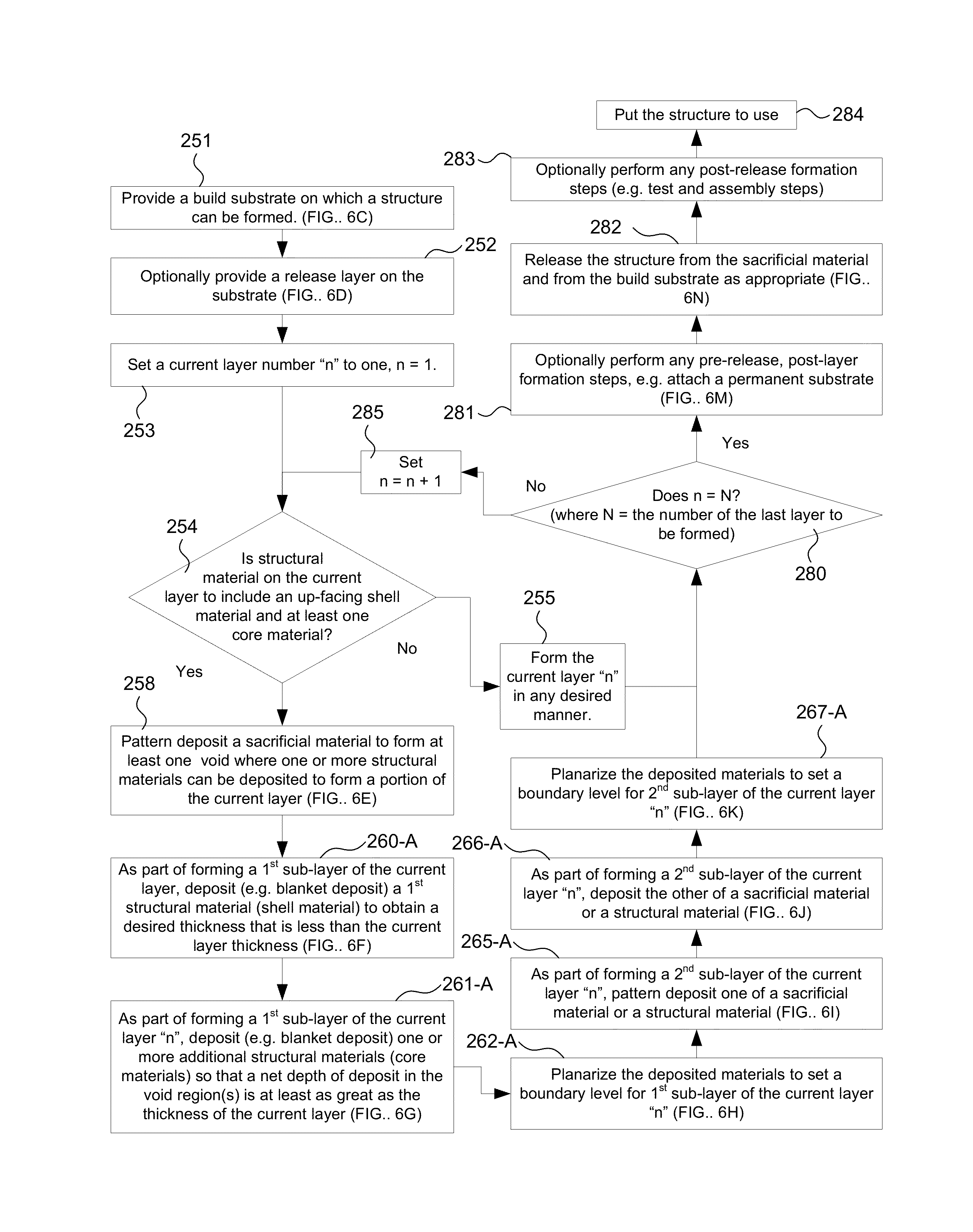
[0145]FIG. 6A provides a flowchart for a process according to the invention where the structure is formed from at least a first structural material that provides a shell material that fully encapsulates at least a second structural material that is a core structural material and may also be a functional structural material and wherein some layers used in forming the structure are compound layers formed of a plurality of stacked sub-layers wherein a first sub-layer of each compound layer provides an up-facing shell structural material and a core structural material and a second sub-layer of each compound layer provides a capping structural material for the core structural material located on the immediately preceding layer, and wherein the sidewalls of the shell may be narrower than a minimum feature size associated with the formation of the layer containing the walls.
[0146]FIG. 6B provides a flowchart for the same process as set forth in FIG. 6A with the exception that instead of vi...
third embodiment
[0165]In a variation of this embodiment, the plating of the capping material (i.e. structural material on a subsequent layer or on the second sub-layer may be by pattern-plating of the structural material, instead of by pattern plating the sacrificial material, followed by blanket plating of the sacrificial material. In some variations (e.g. when the cap is made thin enough, e.g. 1-2 microns in thickness, the plating of the sacrificial material and the planarizing of the cap layer may become unnecessary. The slight topography induced by patterned plating of the capping material may not significantly interfere with fabrication of a next layer. In such variations the plating of the capping material may be considered part of the formation of the previously layer that takes the otherwise planar layer slightly out of planarity but at a level that does not impact the normal formation of a next layer. This variation is, in part, the subject of the third embodiment that will be discussed he...
PUM
| Property | Measurement | Unit |
|---|---|---|
| temperature | aaaaa | aaaaa |
| thicknesses | aaaaa | aaaaa |
| thicknesses | aaaaa | aaaaa |
Abstract
Description
Claims
Application Information