Electrochemical Fabrication Process for Forming Multilayer Multimaterial Microprobe Structures

a technology of microprobe structure and fabrication process, which is applied in the direction of liquid/solution decomposition chemical coating, coating, instruments, etc., can solve the problem of destructive separation of masking material from substra

Inactive Publication Date: 2009-12-31
UNIV OF SOUTHERN CALIFORNIA
View PDF59 Cites 2 Cited by
  • Summary
  • Abstract
  • Description
  • Claims
  • Application Information

AI Technical Summary

Benefits of technology

[0033]It is an object of some embodiments of the invention to provide an enh

Problems solved by technology

The CC mask plating process is distinct from a “through-mask” plating process in that in a through-mas

Method used


Image

  • Electrochemical Fabrication Process for Forming Multilayer Multimaterial Microprobe Structures
  • Electrochemical Fabrication Process for Forming Multilayer Multimaterial Microprobe Structures
  • Electrochemical Fabrication Process for Forming Multilayer Multimaterial Microprobe Structures

Examples


Embodiment Construction

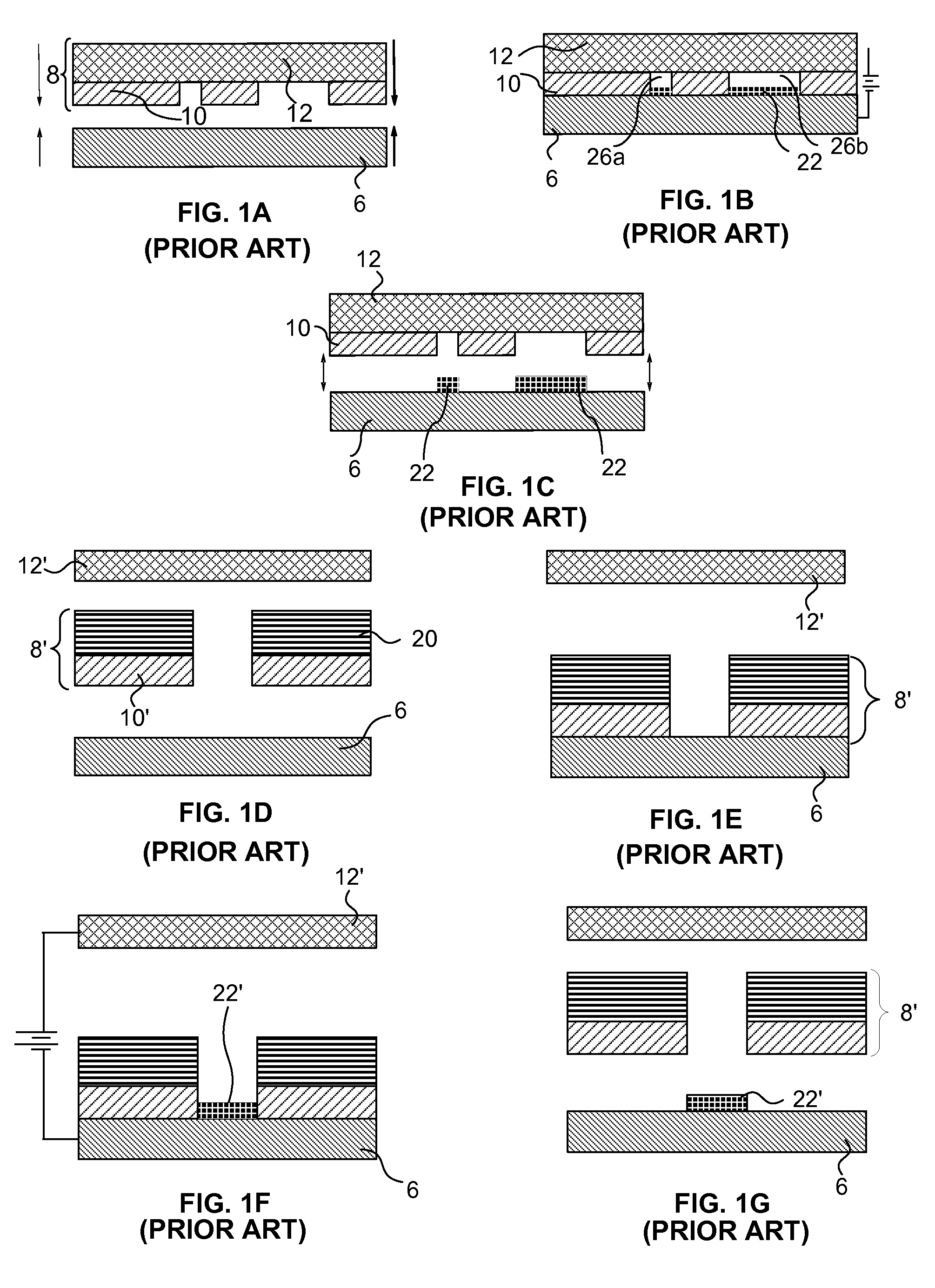
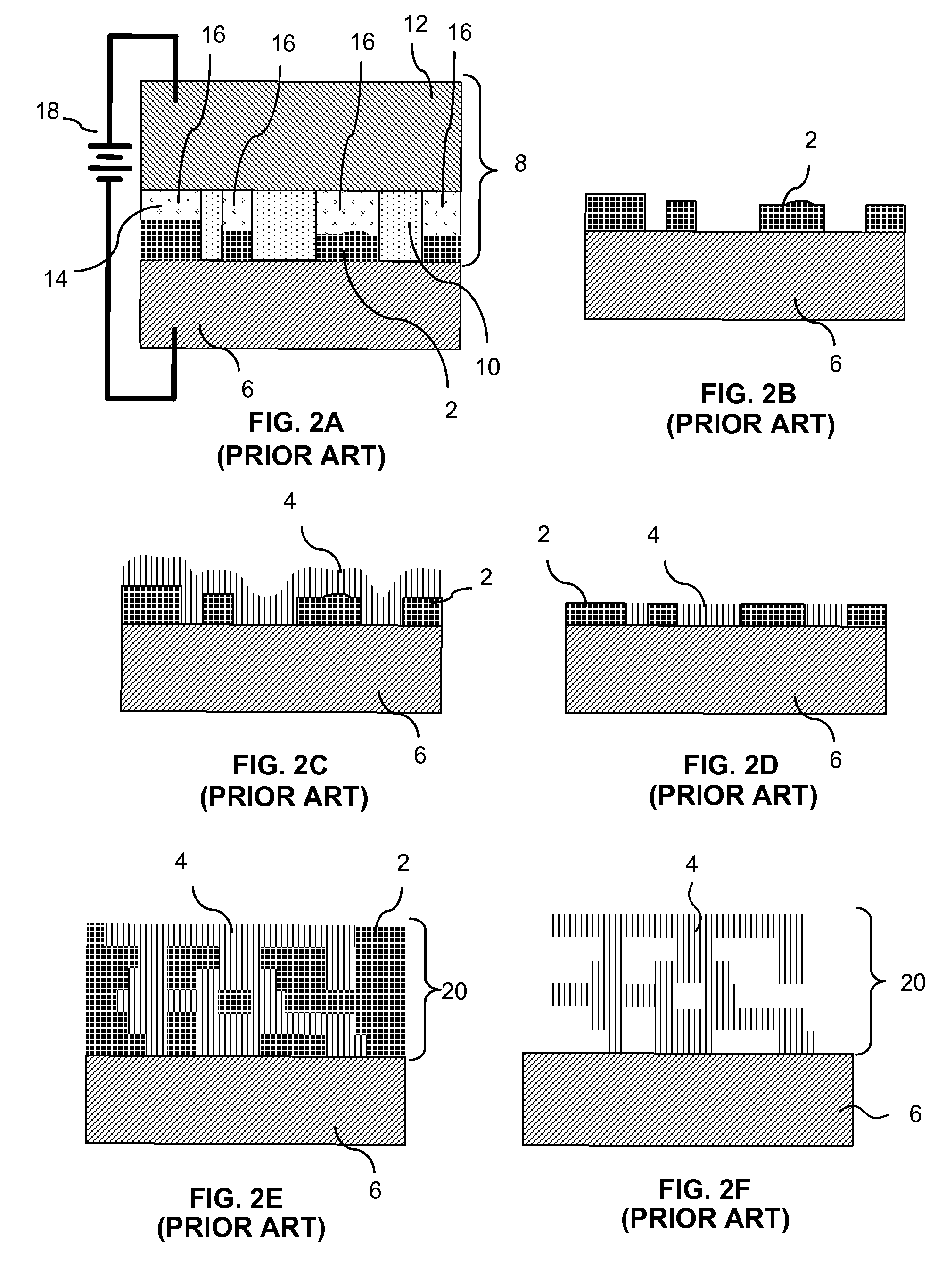
[0050]FIGS. 1A-1G, 2A-2F, and 3A-3C illustrate various features of one form of electrochemical fabrication that are known. Other electrochemical fabrication techniques are set forth in the '630 patent referenced above, in the various previously incorporated publications, in various other patents and patent applications incorporated herein by reference, still others may be derived from combinations of various approaches described in these publications, patents, and applications, or are otherwise known or ascertainable by those of skill in the art from the teachings set forth herein. All of these techniques may be combined with those of the various embodiments of various aspects of the invention to yield enhanced embodiments. Still other embodiments may be derived from combinations of the various embodiments explicitly set forth herein.

[0051]FIGS. 4A-4I illustrate various stages in the formation of a single layer of a multi-layer fabrication process where a second metal is deposited o...


PUM

PropertyMeasurementUnit
Dielectric polarization enthalpyaaaaaaaaaa

Abstract

Some embodiments of the invention are directed to the electrochemical fabrication of microprobes which are formed from a core material and a material that partially coats the surface of the probe. Other embodiments are directed to the electrochemical fabrication of microprobes which are formed from a core material and a material that completely coats the surface of each layer from which the probe is formed including interlayer regions. These first two groups of embodiments incorporate both the core material and the coating material during the formation of each layer. Still other embodiments are directed to the electrochemical fabrication of microprobe arrays that are partially encapsulated by a dielectric material during a post layer formation coating process. In even further embodiments, the electrochemical fabrication of microprobes from two or more materials may occur by incorporating a coating material around each layer of the structure without locating the coating material in inter-layer regions.

Description

RELATED APPLICATIONS[0001]This application is a continuation of U.S. patent application Ser. No. 11 / 029,211 (Microfabrica docket number P-US138-A-MF), filed Jan. 3, 2005 which claims benefit to U.S. Provisional Patent Application Nos. 60 / 533,897, 60 / 533,975, 60 / 533,947, 60 / 533,948, each filed on Dec. 31, 2003; and to 60 / 540,510, filed Jan. 29, 2004; this application is also a CIP of U.S. patent application Ser. No. 10 / 949,738 (Microfabrica docket P-US119-A-MF), filed Sep. 24, 2004 which in turn is a CIP of Ser. No. 10 / 772,943 (Microfabrica docket P-US097-A-MF), which in turn claims benefit of U.S. App. Nos. 60 / 445,186; 60 / 506,015; 60 / 533,933, and 60 / 536,865; furthermore the '738 application claims benefit of U.S. App. Nos. 60 / 506,015; 60 / 533,933; and 60 / 536,865. Each of these applications, including any appendices attached thereto, is incorporated herein by reference as if set forth in full herein.FIELD OF THE INVENTION[0002]The present invention relates generally to the field of El...

Claims


Application Information

Patent Timeline
IPC IPC(8): B32B37/00B32B38/10
CPCG01R1/06716G01R1/06744G01R1/06755C23C18/1651H01L21/4853C25D1/003C23C18/1605G01R3/00C25D5/10C25D5/02
Inventor COHEN, ADAM L.KUMAR, ANANDA H.LOCKARD, MICHAEL S.SMALLEY, DENNIS R.
Owner UNIV OF SOUTHERN CALIFORNIA
Why Eureka
Try Eureka