Unlock instant, AI-driven research and patent intelligence for your innovation.

Semiconductor device and manufacturing method thereof

Active Publication Date: 2016-09-15
SK HYNIX INC
View PDF0 Cites 17 Cited by
  • Summary
  • Abstract
  • Description
  • Claims
  • Application Information

AI Technical Summary

Benefits of technology

The patent describes a semiconductor device and a method for manufacturing it. The device includes a cell region and contact regions located at both sides of the cell region. The device also includes a first source layer and a second source layer. A reinforcement pattern is formed in the second source layer, and a stacked structure including conductive layers and insulating layers alternately stacked over the second source layer and the reinforcement pattern is also included. Channel layers and memory layers are formed in the device. The method includes steps for forming a sacrificial layer, forming a reinforcement pattern in the sacrificial layer, and forming a stacked structure over the sacrificial layer. A source layer is also included in the method. The technical effect of the patent is to provide a semiconductor device with a reinforcement pattern that enhances its stability and reliability, and a method for manufacturing it.

Problems solved by technology

Two-dimensional memory devices having memory cells fabricated in a single layer over a silicon substrate have reached their limits when it comes to increasing their degree of integration.
However, as the height of the stacked structure increases, it may be more difficult to perform an etch process and form a source layer coupled to the memory string.
In addition, the memory cells stacked on each other may have non-uniform characteristics due to processing limitations.

Method used


Image

  • Semiconductor device and manufacturing method thereof
  • Semiconductor device and manufacturing method thereof
  • Semiconductor device and manufacturing method thereof

Examples


Embodiment Construction

[0028]Hereinafter, various embodiments will be described in detail with reference to the accompanying figures. In the figures, thicknesses and lengths of components may be exaggerated for convenience of illustration. In the following description, a detailed explanation of related functions and constitutions may be omitted for simplicity and conciseness. Like reference numerals refer to like elements throughout the specification and figures. Various embodiments are directed to a semiconductor device that is easy to manufacture and has improved characteristics, and a manufacturing method thereof.

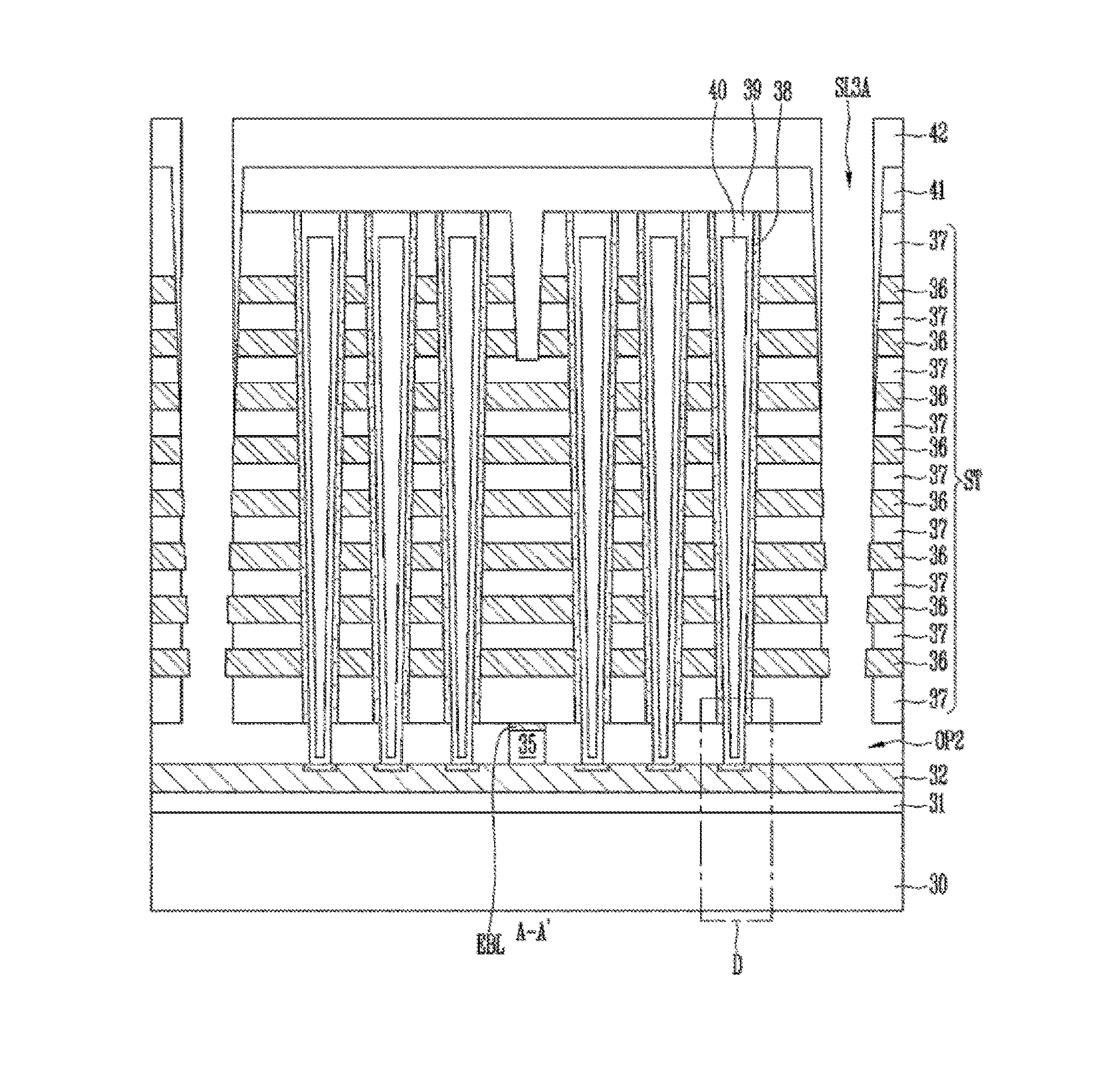
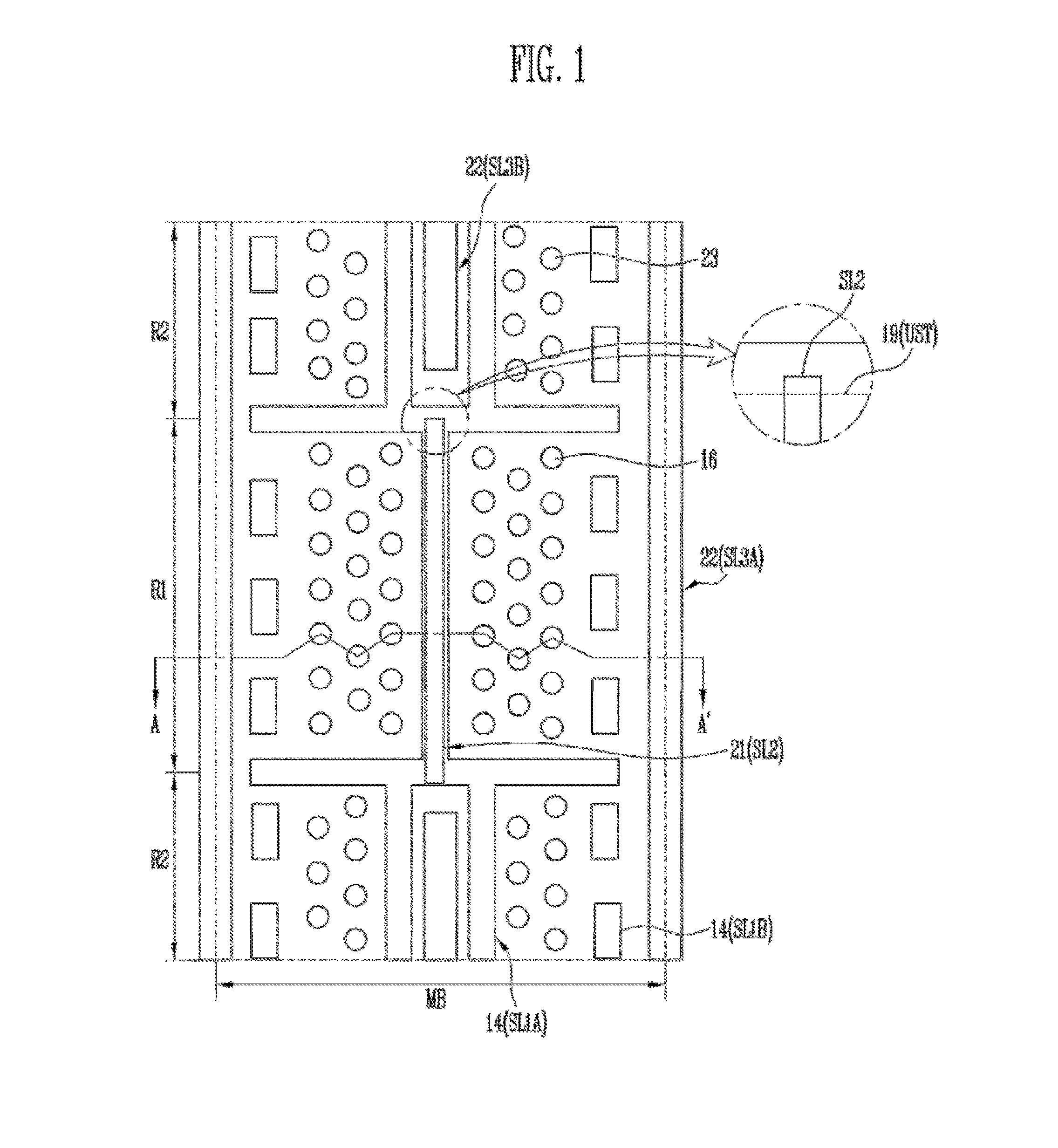
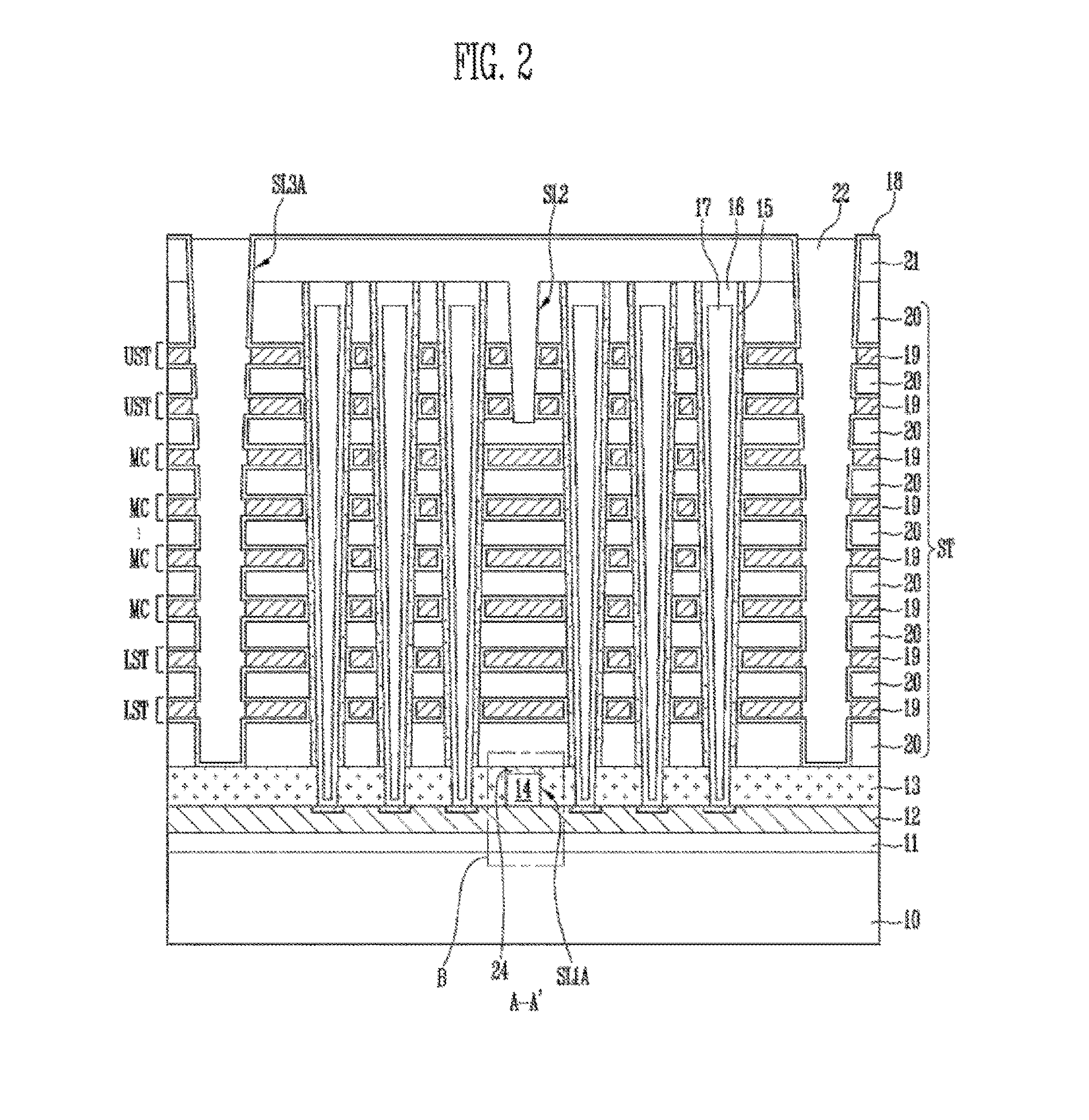
[0029]Referring to FIGS. 1 and 2, a layout view and a cross-sectional view of the structure of a semiconductor device according to an embodiment, respectively are illustrated. FIG. 2 is a cross-sectional view taken along line A-A′ of FIG. 1.

[0030]In FIGS. 1 and 2, a semiconductor device according to an embodiment may include a substrate 10, a first source layer 12, a second source layer 13, a ...


PUM


Abstract

A semiconductor device includes a substrate in which a cell region and contact regions located at both sides of the cell region are defined, a first source layer formed over the substrate, a second source layer formed over the first source layer, a reinforcement pattern formed in the second source layer, a stacked structure including conductive layers and insulating layers alternately stacked over the second source layer and the reinforcement pattern, channel layers passing through the stacked structure and the second source layer and electrically coupled to the second source layer, and an isolation insulating pattern passing through at least one top conductive layer of the conductive layers.

Description

CROSS-REFERENCE TO RELATED APPLICATION[0001]The present application claims priority to Korean patent application number 10-2015-0033817, filed on Mar. 11, 2015 and Korean patent application number 10-2015-0054732, filed on Apr. 17, 2015, the entire disclosures of which are herein incorporated by reference in their entirety.BACKGROUND[0002]1. Field of Invention[0003]Various embodiments relate generally to an electronic device and a manufacturing method thereof, and more particularly, to a semiconductor device having a three-dimensional structure and a manufacturing method thereof.[0004]2. Description of Related Art[0005]Non-volatile memory devices retain stored data in the absence of a power supply. Two-dimensional memory devices having memory cells fabricated in a single layer over a silicon substrate have reached their limits when it comes to increasing their degree of integration. Accordingly, three-dimensional non-volatile memory devices having memory cells stacked in a vertical ...

Claims


Application Information

Patent Timeline
IPC IPC(8): H01L27/115
CPCH01L27/115H01L27/11504H01L27/11507H01L27/2481H10B63/30H10B63/34H10B63/845H10N70/25H10N70/20H10N70/823H10N70/231H10N70/883H10N70/011H10B43/10H10B43/35H10B43/27H10B53/10H10B53/30H10B63/84
Inventor LEE, KI HONGPYI, SEUNG HO
Owner SK HYNIX INC
Features
  • R&D
  • Intellectual Property
  • Life Sciences
  • Materials
  • Tech Scout
  • Unparalleled Data Quality
  • Higher Quality Content
  • 60% Fewer Hallucinations
Learn More