
Image forming device, control method for image forming device, and control program for image forming device

Active Publication Date: 2016-12-15
KONICA MINOLTA INC
View PDF4 Cites 2 Cited by
  • Summary
  • Abstract
  • Description
  • Claims
  • Application Information

AI Technical Summary

Benefits of technology

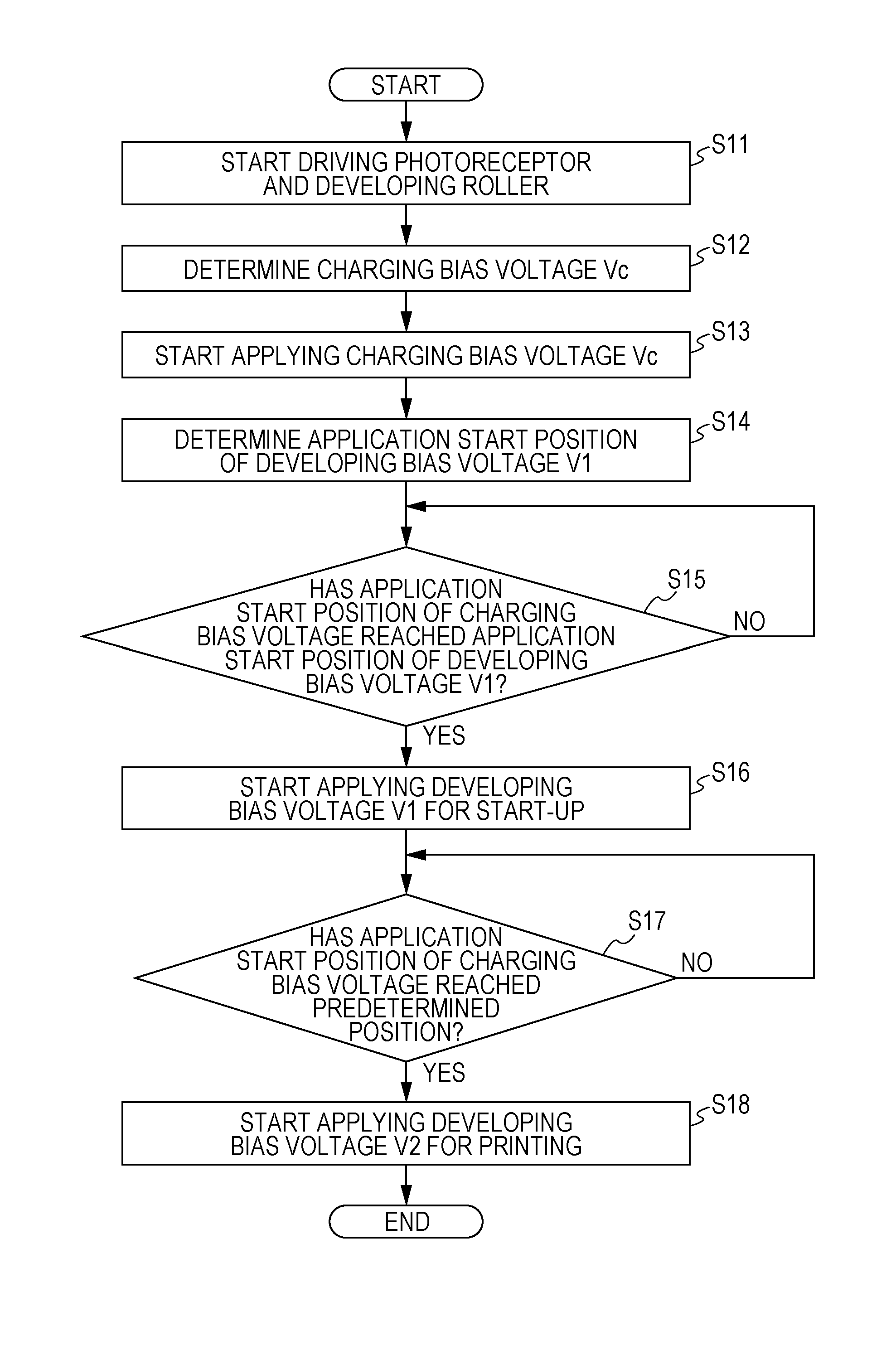
The present invention relates to an image forming device, method, and program that can prevent carrier adhesion to the image carrying body while reducing toner consumption. This is achieved by applying a developing bias voltage in a stepwise manner and using a computer program to determine the optimal value of the charging bias voltage during image formation. By controlling the timing to start applying the developing bias voltage, the method ensures that the larger the charging bias voltage, the sooner it is applied, and the smaller the charging bias voltage, the longer it is applied. This results in a more efficient and effective development process, leading to improved image quality and reduced costs.

Problems solved by technology

In the case where image forming is performed by the two-component development system, malfunction may occur when the toner or the carrier grossly adheres to a portion immediately before an image area on an image carrying body.
When the flaw is made on the cleaning blade, cleaning failure may occur on the image carrying body later due to the portion having the flaw, and a black stripe may appear on a formed image.
Carrier adhesion to the transfer member may cause transfer failure at the time of transferring a toner image to a transfer material (such as paper and an intermediate transfer belt) from the image carrying body next time.
When the toner adheres to the transfer member, an abnormality such as marking back on a transfer material may be caused at the time of transferring a toner image to the transfer material next time.
Particularly, when a transfer roller made of a foamed sponge having an uneven surface is used as the transfer member, the problem of toner adhesion is apparent.
The malfunction caused by carrier adhesion gives more damage on an image forming device.
Therefore, when design is made so as not to cause carrier adhesion under any kinds of conditions, there may be a problem that a toner adhesion amount is increased.
In contrast, when the timing to start applying the developing bias voltage is thus set early conform to the case of having the wide charging range, there maybe a problem in which a toner consumption amount is increased in the case of having a narrow charging range.
These problems are apparent especially in an image forming device in which the surface of the image carrying body is charged by a discharging phenomenon, such as a roller charging system in which direct current bias voltage (DC bias voltage) is applied as the charging bias voltage.
More specifically, when design is made such that application of the developing bias voltage is started early conforming to a case of performing relatively intense discharge in order to prevent carrier adhesion, a toner consumption amount may be increased in the case of performing relatively weak discharge.

Method used


Image

  • Image forming device, control method for image forming device, and control program for image forming device
  • Image forming device, control method for image forming device, and control program for image forming device
  • Image forming device, control method for image forming device, and control program for image forming device

Examples


embodiment

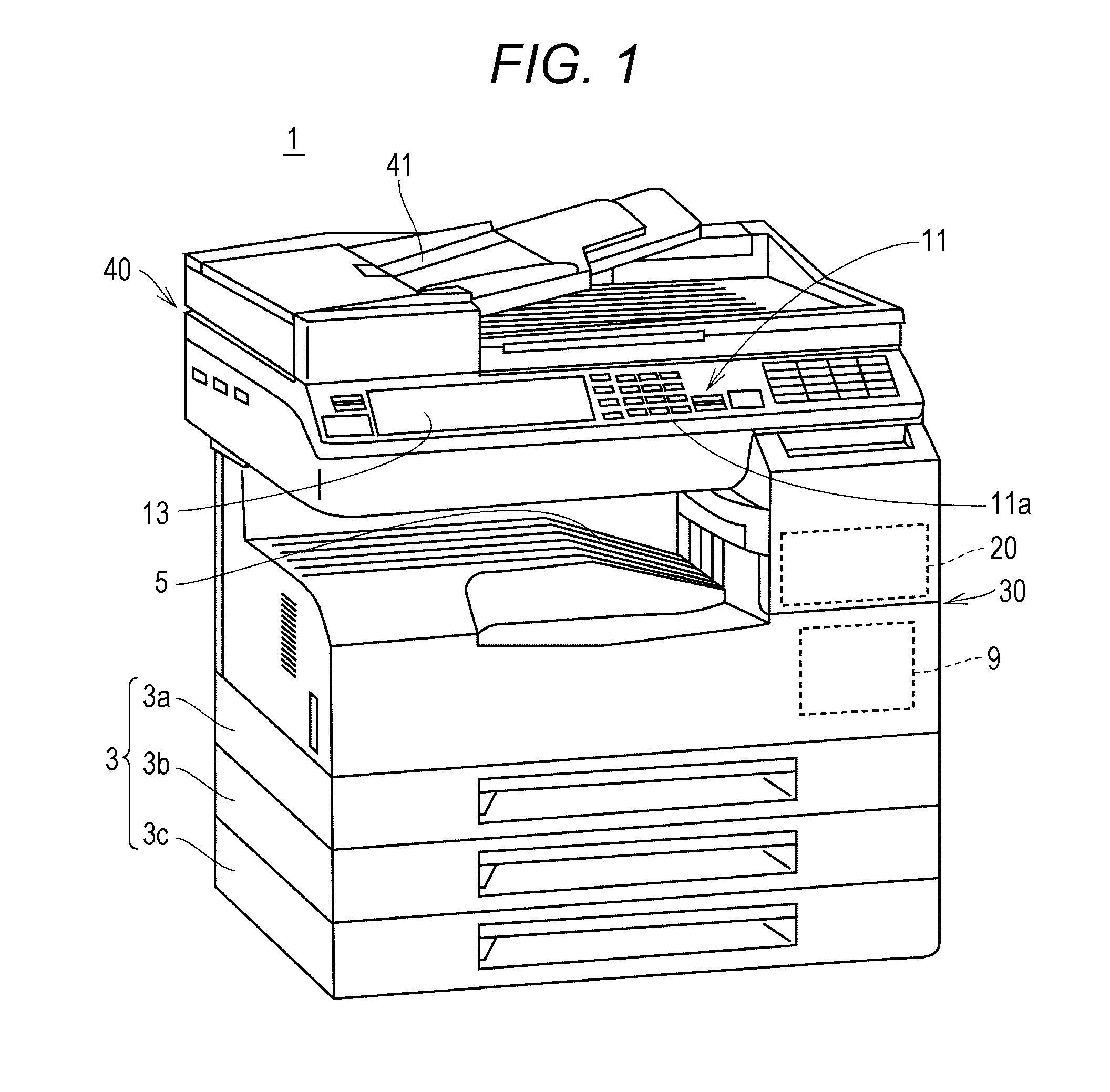
[0045]FIG. 1 is a perspective view illustrating an image forming device according to an embodiment of the present invention.

[0046][Structure of Image Forming Device 1]

[0047]As illustrated in FIG. 1, an image forming device 1 includes a paper feeding cassette 3, a paper discharging tray 5, a power supply unit 9, an operating unit 11, a controller (an exemplary control unit) 20, a printing unit 30, and a scanning unit 40. The controller 20 includes a CPU 21 and the like as described later (refer to FIG. 4). The controller 20 and the printing unit 30 are disposed inside a housing of the image forming device 1.

[0048]The image forming device 1 includes three paper feeding cassettes 3 (paper feeding cassettes 3a, 3b, 3c). In the respective paper feeding cassettes 3, for example, papers having sizes different from each other are preloaded (such as B5 size, A4 size, and A3 size). The paper feeding cassettes 3 are disposed at a lower portion of the image forming device 1 in a manner insertab...


PUM


Abstract

An image forming device includes: a charging unit configured to apply charging bias voltage to a charging member and charge a surface of an image carrying body; an exposure unit configured to expose the surface of the image carrying body, and form an electrostatic latent image; a developing unit configured to apply developing bias voltage to a developer carrying body, and develop the electrostatic latent image; and a control unit configured to control timing to start applying the developing bias voltage relative to timing to start applying the charging bias voltage, wherein the control unit performs control such that the larger an absolute value of the charging bias voltage is, the shorter an interval from timing to start applying the charging bias voltage to timing to start applying the developing bias voltage becomes, and such that the smaller the absolute value is, the longer the interval becomes.

Description

[0001]The entire disclosure of Japanese Patent Application No. 2015-116952 filed on Jun. 9, 2015 including description, claims, drawings, and abstract are incorporated herein by reference in its entirety.BACKGROUND OF THE INVENTIONField of the Invention[0002]The present invention relates to an image forming device, a control method for the image forming device, and a control program for the image forming device, and particularly relates to an image forming device that forms an image on a paper by electrophotography, a control method for the image forming device, and a control program for the image forming device.Description of the Related Art[0003]An electrophotographic image forming device is widely used for such purposes as a multi-function peripheral (MFP) having a scanner function, a facsimile function, a copy function, a function as a printer, a data communication function, and a server function, a facsimile machine, a copy machine, and a printer.[0004]In the electrophotographi...

Claims


Application Information

Patent Timeline
IPC IPC(8): G03G15/02G03G15/06
CPCG03G15/065G03G15/0266G03G15/0283G03G21/14
Inventor NAKAYAMA, KANJIYOSHIMOTO, SHINICHIKANDA, JUNJIINADA, YASUYUKIMANDAI, YUUSUKEMUKOBAYASHI, YU
Owner KONICA MINOLTA INC
Learn More