Supercharge Your Innovation With Domain-Expert AI Agents!

Array substrate, display panel and display device containing the same

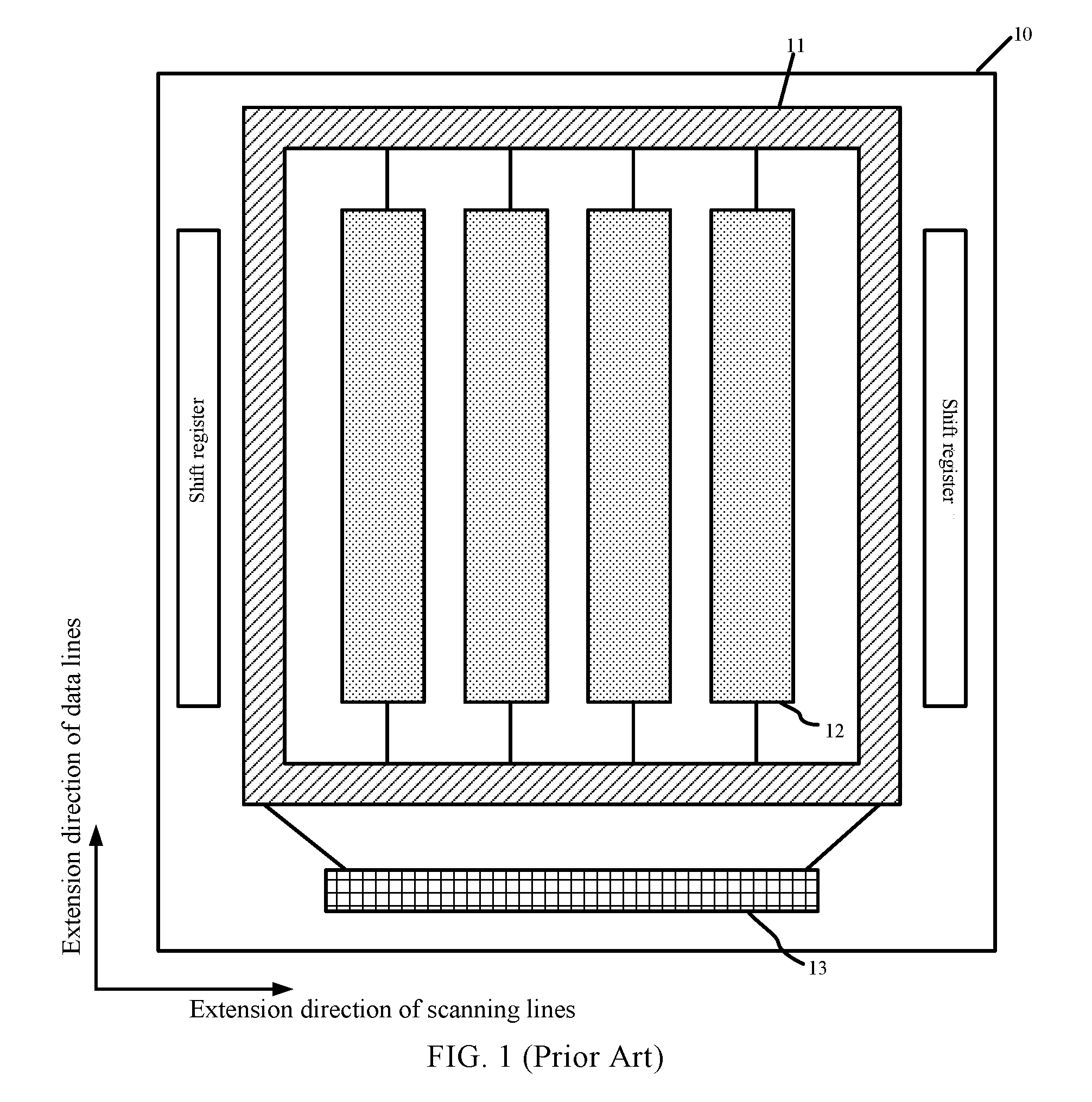
a display panel and substrate technology, applied in the field of display technology, can solve the problems of lowering touch-control sensitivity, and the portion of the common voltage signal line b>11/b> that is parallel to the shift register may not be beneficial for the narrowing of the display panel fram

Active Publication Date: 2017-02-02
XIAMEN TIANMA MICRO ELECTRONICS +1
View PDF5 Cites 1 Cited by
  • Summary
  • Abstract
  • Description
  • Claims
  • Application Information

AI Technical Summary

Benefits of technology

The present patent provides an array substrate for display panels, which has stripe-shaped first electrodes and a first metal electrode. The integrated circuit and the metal electrode are placed on the same side of the display area and connected through a signal line. This design ensures a common voltage signal to the first electrode during display periods, resulting in improved display quality and stability.

Problems solved by technology

Between the shift registers and the portion of common voltage signal line 11 that is parallel to the shift registers, coupling capacitances may form and consume touch-control induced charges, thus lowering touch-control sensitivity.
Further, the portion of the common voltage signal line 11 that is parallel to the shift registers may not be beneficial for the narrowing of the display panel frame.

Method used


Image

  • Array substrate, display panel and display device containing the same
  • Array substrate, display panel and display device containing the same
  • Array substrate, display panel and display device containing the same

Examples


Embodiment Construction

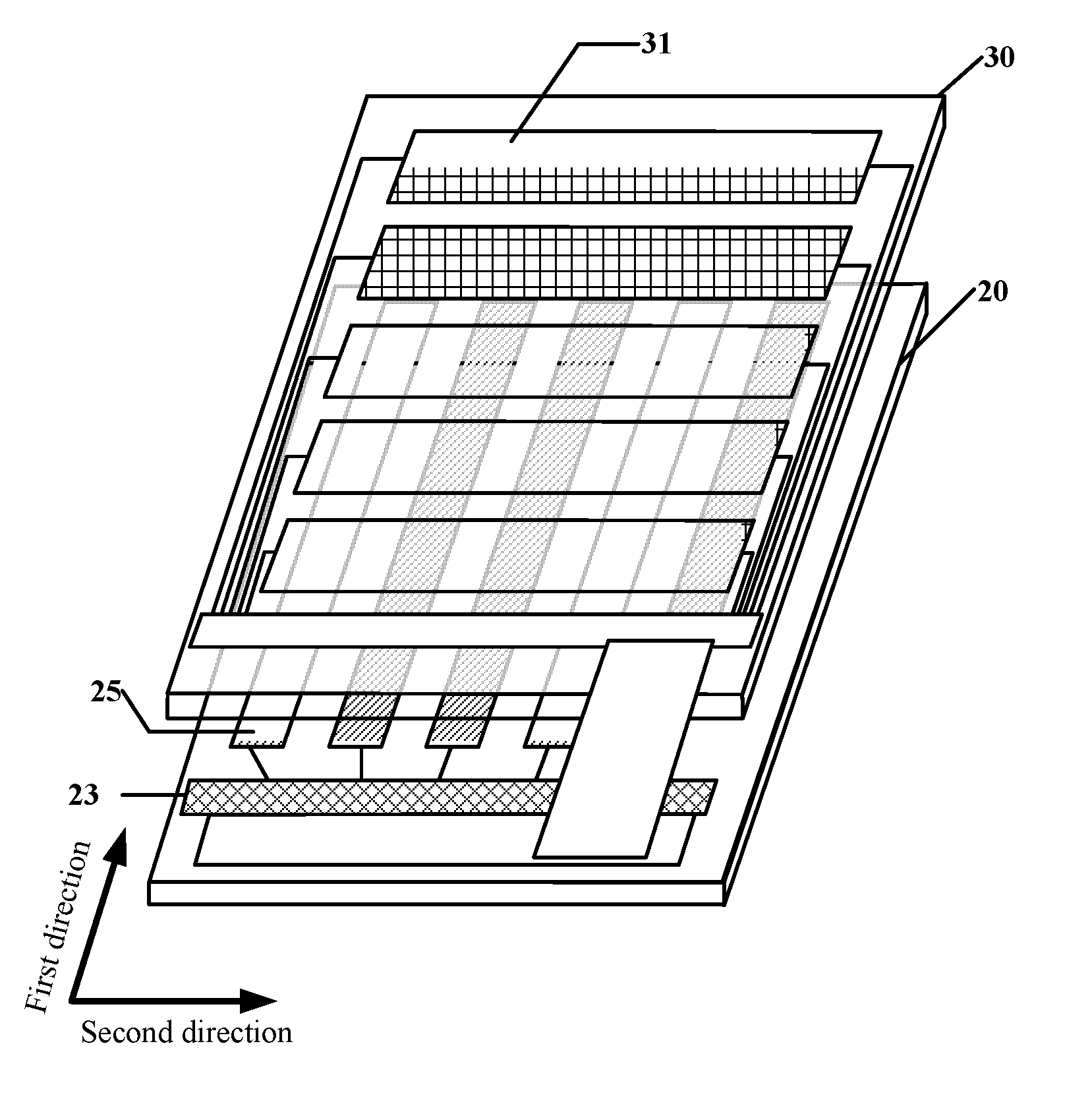
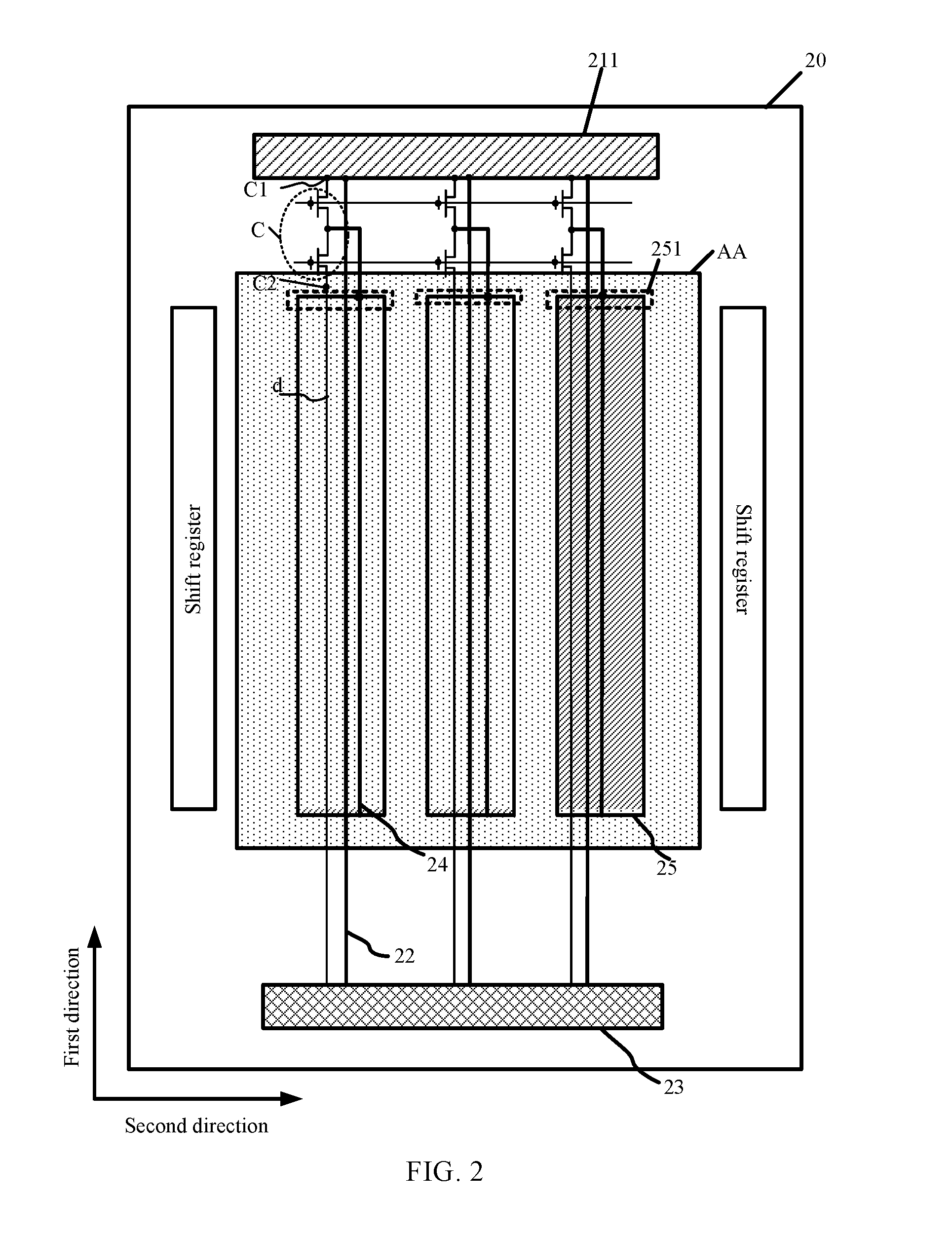
[0020]Reference will now be made in detail to exemplary embodiments of the invention, which are illustrated in the accompanying drawings. Hereinafter, embodiments consistent with the disclosure will be described with reference to drawings. Wherever possible, the same reference numbers will be used throughout the drawings to refer to the same or like parts. It is apparent that the described embodiments are some but not all of the embodiments of the present invention. Based on the disclosed embodiments, persons of ordinary skill in the art may derive other embodiments consistent with the present disclosure, all of which are within the scope of the present invention. Further, in the present disclosure, the disclosed embodiments and the features of the disclosed embodiments may be combined or separated under conditions without conflicts.

[0021]As discussed above, in existing mutual capacitive touch-control liquid crystal display panels, a portion of common voltage signal line that is par...


PUM

PropertyMeasurementUnit
widthaaaaaaaaaa
voltageaaaaaaaaaa
Currentaaaaaaaaaa

Abstract

An array substrate, a display panel and a display device are provided. The array substrate comprises a plurality of stripe-shaped first electrodes extending along a first direction and arranged along a second direction, an integrated circuit, and a first metal electrode. An extension direction of the integrated circuit is parallel to the second direction. An extension direction of the first metal electrode is parallel to the second direction. The first metal electrode and the integrated circuit are disposed on two opposite sides of the display area, respectively, and the first metal electrode is electrically connected to at least one first signal line via the integrated circuit. Each first electrode includes a first end close to the first metal electrode. The first metal electrode is electrically connected to the first end to provide a common voltage signal to the first electrode during a display period.

Description

CROSS-REFERENCES TO RELATED APPLICATIONS[0001]This application claims priority of Chinese Patent Application No. 201610617471.6, filed on Jul. 29, 2016, the entire contents of which are hereby incorporated by reference.FIELD OF THE INVENTION[0002]The present disclosure generally relates to the field of display technology including touch-control display technology and, more particularly, relates to an array substrate, a display panel and a display device containing the same.BACKGROUND[0003]Current mutual capacitive touch-control liquid crystal display panels often divide a common electrode into a plurality of mutually-insulated stripe-shaped sub-common electrodes. A time-sharing multiplexing method is applied, and sub-common electrodes are treated as common electrodes during a display period and multiplexed as touch-control electrodes during a touch-control period. FIG. 1 illustrates an array substrate in an existing touch-control display panel.[0004]As shown in FIG. 1, an array subs...

Claims


Application Information

Patent Timeline
Patent Type & Authority Applications(United States)
IPC IPC(8): G06F3/041G02F1/1343G02F1/1333G02F1/1335G02F1/1345G06F3/044G02F1/1362
CPCG06F3/0416G06F3/0412G06F3/044G02F1/13338G02F1/136286G02F1/133514G02F1/13454G02F1/134309G06F3/0446G06F3/0445G06F3/04184G02F1/134318
Inventor ZOU, LONGSHENGPAN, CHAOHUANGWANG, ZHIJIEWU, SHUMAO
Owner XIAMEN TIANMA MICRO ELECTRONICS
Features
  • R&D
  • Intellectual Property
  • Life Sciences
  • Materials
  • Tech Scout
  • Unparalleled Data Quality
  • Higher Quality Content
  • 60% Fewer Hallucinations
Learn More