Unlock instant, AI-driven research and patent intelligence for your innovation.

Electroluminescent display panel and driving method thereof

a technology of electroluminescent display panel and driving method, which is applied in the direction of instruments, static indicating devices, etc., can solve the problem that the pixels are not able to display correct images

Active Publication Date: 2017-04-13
AU OPTRONICS CORP
View PDF2 Cites 2 Cited by
  • Summary
  • Abstract
  • Description
  • Claims
  • Application Information

AI Technical Summary

Problems solved by technology

However, according to the above arrangement, if time for charging the pixel by data signals is not long enough, a current I flowing through a light emitting element 100 can not reach a predetermined value, such that the pixel is not able to display correct images.

Method used


Image

  • Electroluminescent display panel and driving method thereof
  • Electroluminescent display panel and driving method thereof
  • Electroluminescent display panel and driving method thereof

Examples


first embodiment

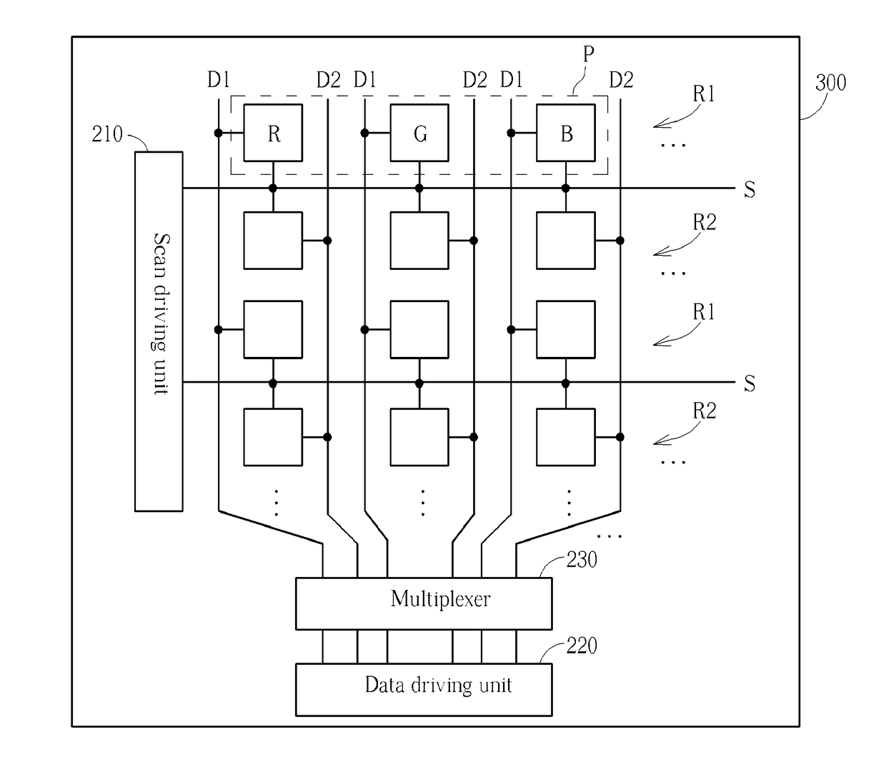
[0025]Please refer to FIG. 2. FIG. 2 is a diagram showing an electroluminescent display panel of the present disclosure. As shown in FIG. 2, the electroluminescent display panel 200 of the present disclosure comprises a plurality of pixels P, a plurality of scan lines S, a plurality of first data lines D1, a plurality of second data lines D2, a scan driving unit 210, and a data driving unit 220. Each of the pixels P comprises a plurality of sub-pixels, such as red sub-pixels R, green sub-pixels G and blue sub-pixels B. Pixel rendering of each of the sub-pixels R, G, B can be like the pixel rendering (such as arrangement of transistors and capacitors) shown in FIG. 1, or other pixel rendering for eliminating influence from different threshold voltage drops of transistors. Each of the scan limes S is electrically connected to a first row R1 of sub-pixels and a second row R2 of sub-pixels of two adjacent rows of sub-pixels. Each of the first data lines D1 is electrically connected to t...

second embodiment

[0030]Please refer to FIG. 6, and refer to FIG. 3 and FIG. 5 as well. FIG. 6 is a diagram showing the multiplexer in FIG. 3. On and off states of switches of the multiplexer in FIG. 6 are also shown in FIG. 5. As shown in figures, the first switches SW1 and second switches SW2 of the multiplexer 230 are respectively and interlacedly coupled between pins of the data driving unit 220 and the first or second data lines D1, D2. Similarly, the multiplexer 230 conducts the first switches SW1 (turns on the first switches SW1) during the first enable period t1 of the scanning period T of each of the scan lines, conducts the second switches SW2 (turns on the second switches SW2) during the second enable period t2 of the scanning period T, and disconnects the data driving unit 220 from the data lines D1, D2 (turns off the first and second switches SW1, SW2) during the disable period tc of the scanning period T.

[0031]According to the above arrangement, the multiplexer in FIG. 6 not only can ac...

third embodiment

[0032]Please refer to FIG. 7 and FIG. 8 together, and refer to FIG. 3 as well. FIG. 7 is a diagram showing the multiplexer in FIG. 3. FIG. 8 is a diagram showing on and off states of switches of the multiplexer in FIG. 7. Arrangement of sub-pixels R, G, B is shown in FIG. 7. The electroluminescent display panel comprises a plurality of sub-pixels, such as green sub-pixels G, red sub-pixels R, and blue sub-pixels B. Wherein one of any three adjacent columns of sub-pixels is a column of green sub-pixels, and the columns of green sub-pixels are not next to each other. As shown in FIG. 7, the first column of sub-pixels is a column of red sub-pixels R, the second column of sub-pixels is a column of green sub-pixels G, and the third column of sub-pixels is a column of blue sub-pixels B. The multiplexer 230 comprises a plurality of first switches SW1, a plurality of second switches SW2, and a plurality of third switches SW3. Each of the first switches SW1 is coupled to one of a first data ...


PUM

PropertyMeasurementUnit
electroluminescentaaaaaaaaaa
brightnessaaaaaaaaaa
threshold voltageaaaaaaaaaa

Abstract

An electroluminescent display panel includes a plurality of sub-pixels; a plurality of scan lines, each of the scan lines being electrically connected to a first row of sub-pixels and a second row of sub-pixels of two adjacent rows; a plurality of first data lines electrically connected to the first rows of sub-pixels of corresponding columns respectively; a plurality of second data lines electrically connected to the second rows of sub-pixels of corresponding columns respectively; a scan driving unit for outputting a plurality of scanning signals; and a data driving unit for outputting a plurality of dada signals; wherein the scanning signals sequentially turn on two adjacent rows of sub-pixels via the scan lines, the data signals on the first data lines charge the first rows of sub-pixels of the corresponding columns, and the data signals on the second data lines charge the second rows of sub-pixels of the corresponding columns.

Description

[0001]This application is a continuation application of co-pending U.S. application Ser. No. 13 / 935,565, filed Jul. 5, 2013, which claims the benefit of Taiwan application Serial No. 101138904, filed Oct. 22, 2012, the disclosure of which is incorporated by reference herein in its entirety.BACKGROUND[0002]1. Technical Field[0003]The present disclosure relates to an electroluminescent display panel, and more particularly, to an electroluminescent display panel capable of improving image uniformity.[0004]2. Description of the Prior Art[0005]An electroluminescent display panel is a display panel configured to control brightness of light emitting elements of sub-pixels for displaying images. When component characteristics of the sub-pixels of the electroluminescent display panel are not uniform, a mura effect may easily occur, so as to affect quality of the displayed images.[0006]Please refer to FIG. 1. FIG. 1 is a diagram showing a pixel of an electroluminescent display panel of the pr...

Claims


Application Information

Patent Timeline
Patent Type & Authority Applications(United States)
IPC IPC(8): G09G3/30
CPCG09G3/30G09G2300/0452G09G2320/0233G09G2310/0297G09G2310/0267G09G2310/0275G09G2310/0251G09G3/3233G09G2300/0426G09G2300/0819G09G2300/0852G09G2300/0861G09G2310/0248G09G2310/0262G09G2320/043
Inventor WANG, TSANG-HONGLAU, CHEE-WAI
Owner AU OPTRONICS CORP