Pixel circuit, display panel, and driving method thereof

a technology of display panel and pixel circuit, which is applied in the direction of electric digital data processing, instruments, computing, etc., can solve the problems of high resolution, large scale, color distortion, and more serious problem of high so as to improve the brightness of middle and low grayscale, improve the effect of color shift and saving costs

Active Publication Date: 2014-07-01
OPTRONIC SCI LLC
View PDF16 Cites 141 Cited by
  • Summary
  • Abstract
  • Description
  • Claims
  • Application Information

AI Technical Summary

Benefits of technology

[0008]Accordingly, the present invention is directed to a display panel, a pixel circuit, and a driving method thereof, capable of effectively improving the frame flicker problem.
[0020]In the structure of the present invention, a complete pixel is divided into two sub-pixels (a first sub-pixel and a second sub-pixel), which is different from the conventional design to improve color shift by increasing gate driver ICs and data driver ICs, thereby saving the cost. Particularly, the driving method of the present invention achieves that the two sub-pixels have two voltages and opposite polarities, thereby further solving the fame flicker problem.

Problems solved by technology

However, the market tends to develop LCDs having wide viewing angle, high resolution, and large scale.
Among them, the technical requirement of the wide viewing angle is originated from the circumstance that when the LCD is viewed at a large viewing angle, a severe color shift of the image occurs, and thus the color is distorted.
The so-called color shift is that when viewing the LCD at a large viewing angle, the frame becomes whiter, that is, the larger viewing angle at the LCD which is viewed results in more serious problem of higher brightness of middle and low grayscale.
However, although the conventional MS pixel structure may effectively solve the circumstance of color shift, the frame flicker may be caused.

Method used


Image

  • Pixel circuit, display panel, and driving method thereof
  • Pixel circuit, display panel, and driving method thereof
  • Pixel circuit, display panel, and driving method thereof

Examples


first embodiment

The First Embodiment

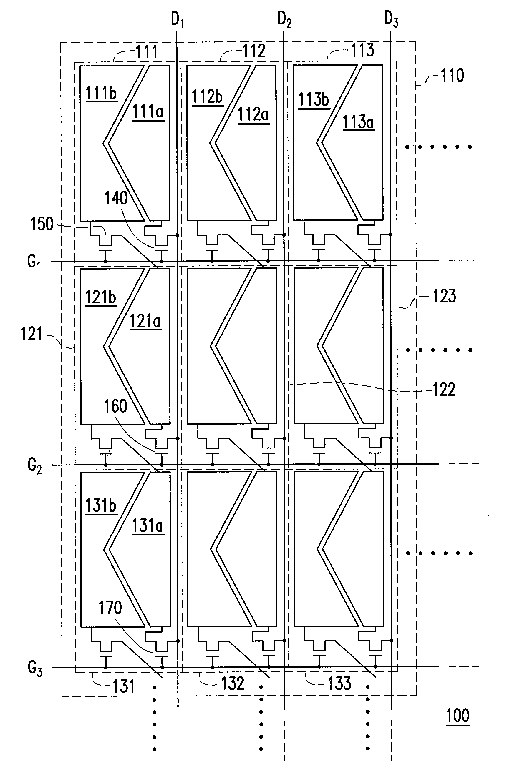
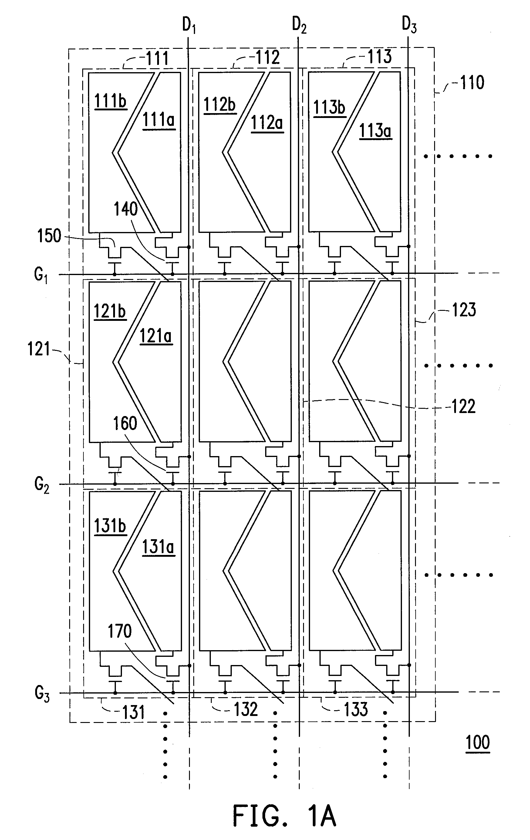
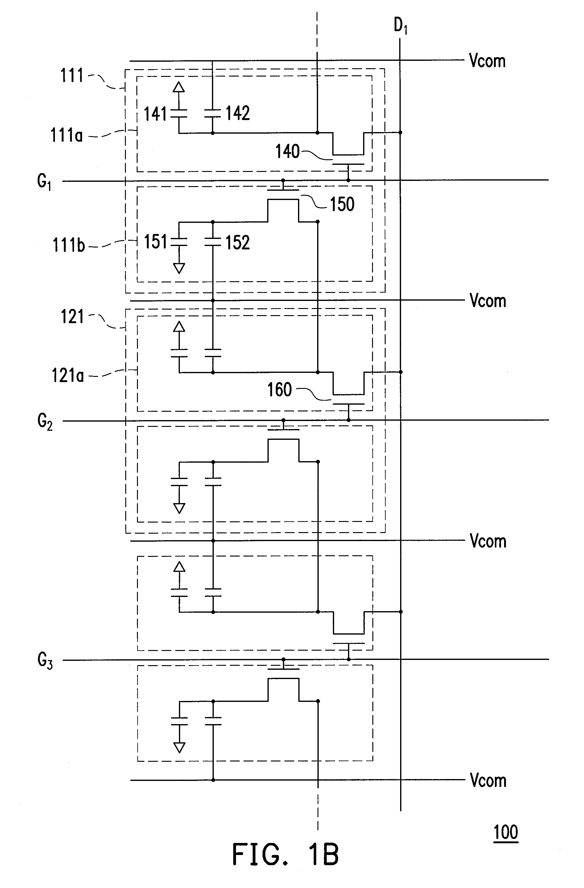
[0036]FIG. 1A is an architecture diagram of a display panel according to the first embodiment of the present invention. Referring to FIG. 1A, the display panel 100 of this embodiment has a plurality of data lines, for example, D1, D2, and D3, and a plurality of scan lines, for example, G1, G2, and G3. The scan lines G1, G2, and G3 . . . are arranged approximately in parallel in a first direction, and the data lines D1, D2, and D3 . . . are arranged approximately in parallel in a second direction. In addition, the scan lines G1, G2, and G3 . . . and the data line D1, D2, and D3 . . . are not intersected.

[0037]The scans line G1, G2, and G3 . . . and the data lines D1, D2, and D3 . . . may enclose a plurality of display regions on the display panel 100, and the display regions are arranged in an array. One pixel is disposed in each display region, thereby forming a pixel array on the display panel 100. Particularly, each pixel is at least divided into a first sub-pi...

second embodiment

The Second Embodiment

[0047]FIG. 6 is an architecture diagram of a display panel according to the second embodiment of the present invention. Referring to FIG. 6, a display panel 600 of this embodiment further includes a first redundant pixel group 601 and a second redundant pixel group 602. The first redundant pixel group 601 may include a plurality of first redundant pixels, and each first redundant pixel may be correspondingly coupled to the pixels in the first row along the first direction respectively. Comparatively, the second redundant pixel group 602 may include a plurality of second redundant pixels, and each second redundant pixel may be correspondingly coupled to the pixels in the last row along the first direction respectively.

[0048]It may be known from the driving method of the first embodiment that the pixels in the last row along the first direction may not be displayed normally unless the second sub-pixels of the pixels in the last row along the first direction are dr...

third embodiment

The Third Embodiment

[0049]The flicker problem has been effectively overcome in the first embodiment. However, in the first embodiment, the polarity of each data signal must be continually switched in the same image, which results in the difficulty in operation. Therefore, an architecture diagram of another display panel as shown in FIG. 7A is provided in the present invention. Referring to FIG. 7A, a display panel 700 of this embodiment is substantially the same as that of the first embodiment, except that in the display panel 700, the first sub-pixels of the pixels in the Nth row along the second direction receive the data signals transmitted on the (N−1)th or the Nth data line. In this embodiment, the first sub-pixels of the pixels in the odd rows receive the data signal transmitted on the (N−1)th data line, and the first sub-pixels of the pixels in the even rows receive the data signal transmitted on the Nth data line. For example, the first sub-pixels 711a and 731a of the pixels...


PUM


Abstract

A pixel circuit includes a first sub-pixel and a second sub-pixel. The first sub-pixel is coupled to a scan line and a data line, so as to determine whether to be enabled according to a first scan signal transmitted on the scan line, and whether to be driven according to a data signal transmitted on the data line. The second sub-pixel is coupled to the scan line, so as to determine whether to be enabled according to the first scan signal. The data signal is in a first state when the first scan signal is in a pre-charged period. The data signal is in a second state during a time interval after the pre-charged period is over and before the first scan signal enters a turn-on period. Voltage polarities of the first state and the second state are opposite. The pixel design can improve color shift and frame flicker.

Description

CROSS-REFERENCE TO RELATED APPLICATION[0001]This application claims the priority benefit of Taiwan application serial no. 97116533, filed on May 5, 2008. The entirety of the above-mentioned patent application is hereby incorporated by reference herein and made a part of specification.BACKGROUND OF THE INVENTION[0002]1. Field of the Invention[0003]The present invention generally relates to a pixel circuit, a display panel, and a driving method thereof, and in particular, to a pixel circuit, a display panel, and a driving method thereof capable of improving color shift and frame flicker.[0004]2. Description of Related Art[0005]Liquid crystal displays (LCDs), having advantages of good space utilization, low power consumption, and no radiation etc., have gradually become mainstream products in the market. However, the market tends to develop LCDs having wide viewing angle, high resolution, and large scale.[0006]Among them, the technical requirement of the wide viewing angle is originate...

Claims


Application Information

Patent Timeline
Patent Type & Authority Patents(United States)
IPC IPC(8): G09G5/00G06F3/038
CPCG09G3/3696G09G2320/0247G09G3/3648G09G2300/0443G09G2300/0426
Inventor CHIEN, CHIH-YUANCHEN, CHIEN-HUAYANG, CHEN-KUOHUANG, HSUEH-YING
Owner OPTRONIC SCI LLC
Why Eureka
Try Eureka