
Semiconductor structure

Active Publication Date: 2017-11-23
MEDIATEK INC
View PDF6 Cites 1 Cited by
  • Summary
  • Abstract
  • Description
  • Claims
  • Application Information

AI Technical Summary

Benefits of technology

The patent is for a semiconductor structure that includes a semiconductor substrate, a well region, an RF circuit, a guard ring, and an isolation region. The well region has a first conductive type and the RF circuit includes a FIN field-effect transistor with first fins and first polys on the well region. The guard ring includes second fins and second polys on the well region. The first fins are arranged parallel to the second fins and are separated from them by the isolation region. The technical effect of this semiconductor structure is to provide better performance and reliability of RF circuits.

Problems solved by technology

In an integrated circuit (IC), one circuit or device will introduce noise that interferes with the operation of other circuits or devices in the IC.
This introduction of noise often degrades the performance of the IC.

Method used


Image

  • Semiconductor structure
  • Semiconductor structure
  • Semiconductor structure

Examples


Embodiment Construction

[0015]The following description is of the best-contemplated mode of carrying out the invention. This description is made for the purpose of illustrating the general principles of the invention and should not be taken in a limiting sense. The scope of the invention is best determined by reference to the appended claims.

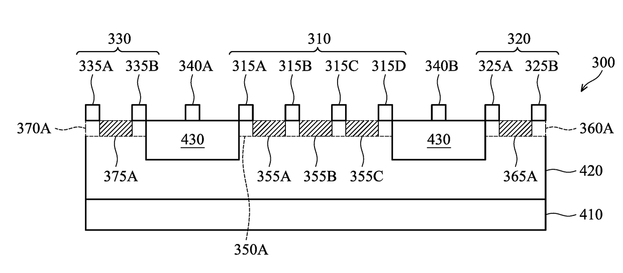
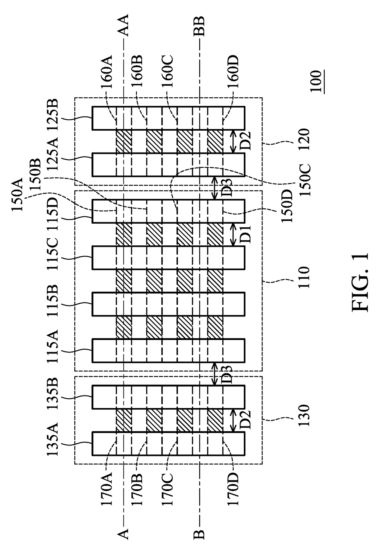
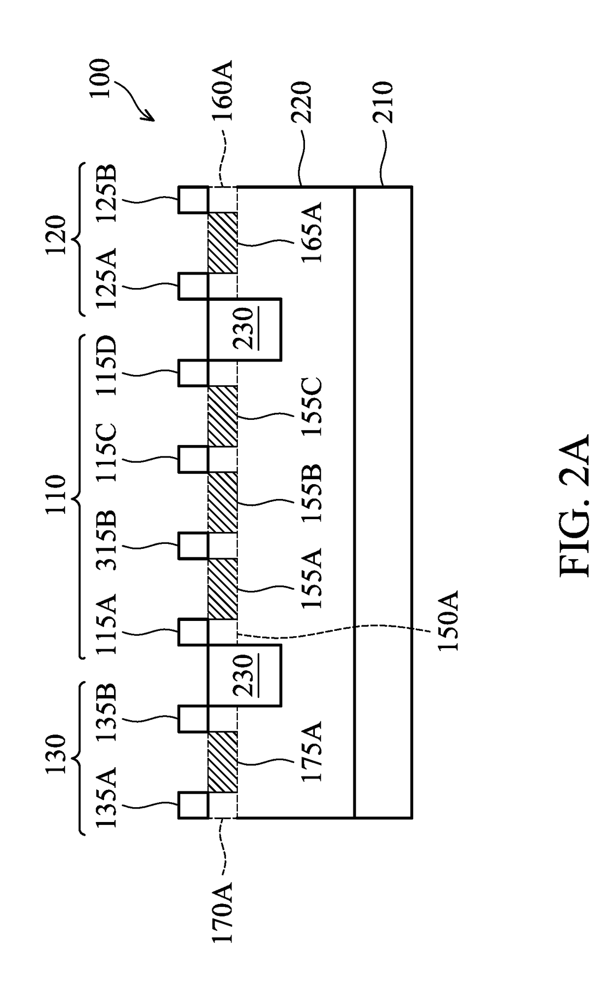
[0016]FIG. 1 shows a semiconductor structure 100 of an integrated circuit (IC) according to an embodiment of the invention. The semiconductor structure 100 comprises a radio frequency (RF) circuit 110, a guard ring 120 disposed on the right side of the RF circuit 110, and a guard ring 130 disposed on the left side of the RF circuit 110. In the RF circuit 110, the RF circuit 110 comprises at least one RF device, and the RF device is a FIN field-effect transistor (FET) formed by a plurality of polys 115A-115D and a plurality of fins 150A-150D. In some embodiments, the RF circuit 110 comprises a plurality of RF devices, and each RF device is a FIN FET. In the RF circuit 1...


PUM


Abstract

A semiconductor structure is provided. The semiconductor structure includes a semiconductor substrate, a well region on the semiconductor substrate, a radio frequency circuit, a first guard ring adjacent to the RF circuit, and a first isolation region directly disposed between the RF circuit and the first guard ring. The well region has a first conductive type. The RF circuit includes a FIN field-effect transistor having a plurality of first fins and a plurality of first polys on the well region, wherein the first polys are perpendicular to the first fins. The first guard ring includes a plurality of second fins and a pair of second polys on the well region, wherein the second polys are perpendicular to the second fins. The first fins are arranged parallel to the second fins, and the first fins are separated from the second fins by the first isolation region.

Description

CROSS REFERENCE TO RELATED APPLICATIONS[0001]This application claims the benefit of U.S. Provisional Application No. 62 / 339,123, filed on May 20, 2016, and U.S. Provisional Application No. 62 / 382,288, filed on Sep. 1, 2016, the entireties of which are incorporated by reference herein.BACKGROUND OF THE INVENTIONField of the Invention[0002]The invention relates to a semiconductor structure, and more particularly to a semiconductor structure of a guard ring for a radio frequency (RF) device.Description of the Related Art[0003]Semiconductor device manufacturers are tasked to deliver products that perform with an expected level of quality. In an integrated circuit (IC), one circuit or device will introduce noise that interferes with the operation of other circuits or devices in the IC. This introduction of noise often degrades the performance of the IC.[0004]Guard rings are used as isolation regions between devices or circuits within an IC. Guard rings surround the devices or circuits of...

Claims


Application Information

Patent Timeline
IPC IPC(8): H01L27/092H01L29/06H01L29/78
CPCH01L27/0924H01L29/0649H01L29/785H01L29/0619H01L23/564H01L27/0886H01L27/0207H01L28/00H01L29/6681
Inventor WANG, YU-JENHUANG, KUO-EN
Owner MEDIATEK INC
Learn More