Wafer level integration including design/co-design, structure process, equipment stress management, and thermal management

a technology of equipment stress management and integration, applied in the direction of semiconductor devices, electrical equipment, semiconductor/solid-state device details, etc., can solve the problems of multi-high function in sub-components and products, heterogeneous product functions, and high manufacturing yield challenges

Active Publication Date: 2018-03-22
IBM CORP
View PDF11 Cites 4 Cited by
  • Summary
  • Abstract
  • Description
  • Claims
  • Application Information

AI Technical Summary

Benefits of technology

[0003]In one embodiment, a method of manufacturing a multi-layer wafer is disclosed. The method comprises applying a stress compensating oxide layer to each of two heterogeneous wafers, applying at least one bonding o

Problems solved by technology

Wafer level integration for heterogeneous product function and multi-high function in sub-component and product is challenging due to different structures, materials, coefficients of ther

Method used


Image

  • Wafer level integration including design/co-design, structure process, equipment stress management, and thermal management
  • Wafer level integration including design/co-design, structure process, equipment stress management, and thermal management
  • Wafer level integration including design/co-design, structure process, equipment stress management, and thermal management

Examples


Embodiment Construction

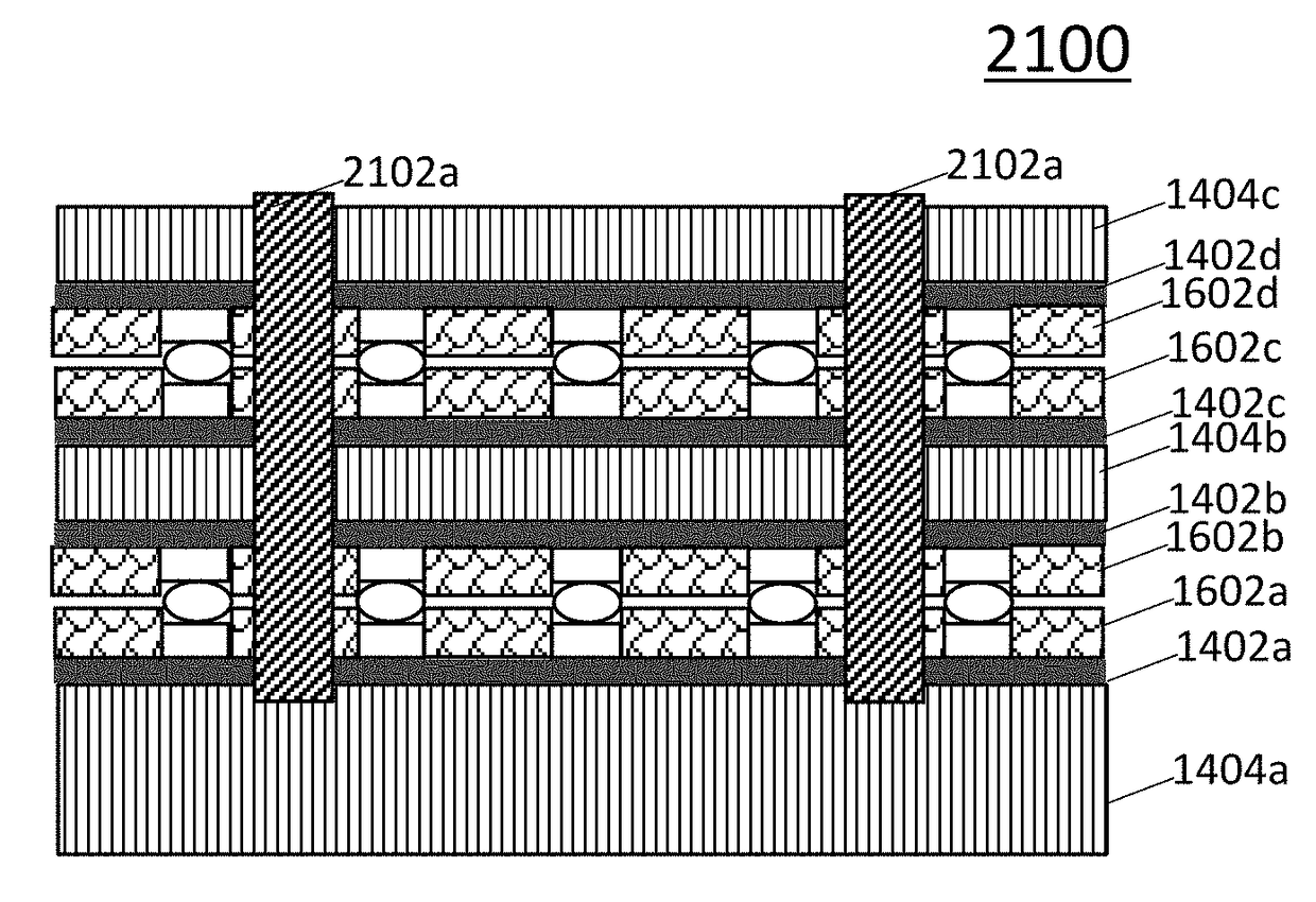
[0027]In this disclosure, methods and structures are provided to support heterogeneous wafer level integration of multi-stack structures to overcome wafer to wafer stress (e.g., mechanical, thermal or other) due to different wafer materials, processes, design, bonding, interconnections or other factors at the wafer and / or die level. These structures and methods reduce stresses between the wafers to minimize warpage during processing and reduce stress in the joined structures in the sub-component, multi-die stack and / or integrated structure for more robust product applications.

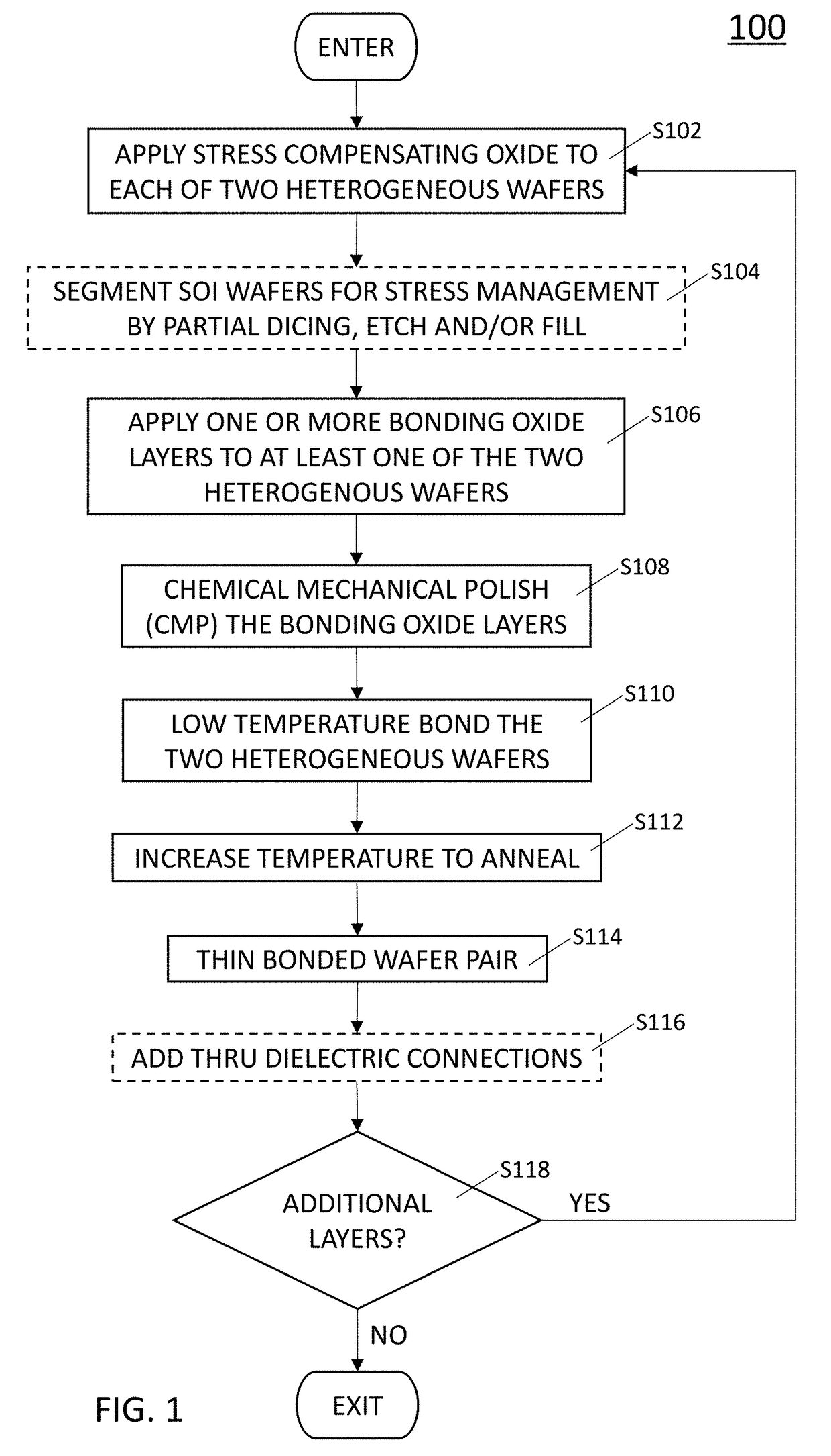
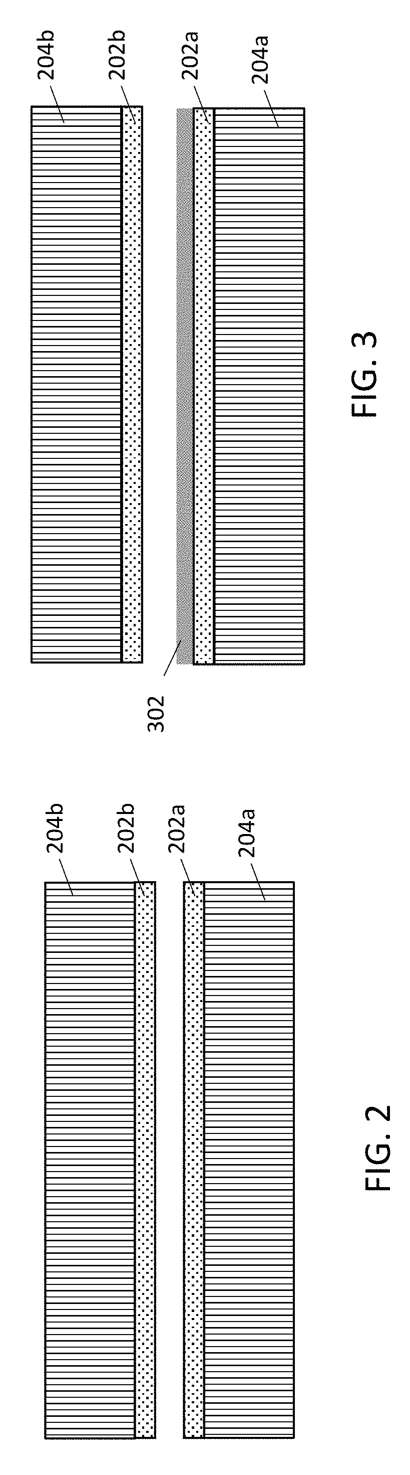
[0028]Referring now to FIG. 1, an operational flowchart 100 is provided which illustrates one example process of manufacturing multi-layer wafers using a stress compensating oxide layer. It should be noted that optional steps of the process 100 are indicated by dashed lines. The process begins by applying, at step S102, a stress compensating oxide layer 202a, 202b (referenced generally herein as “stress compens...


PUM


Abstract

A multi-layer wafer and method of manufacturing such wafer are provided. The method comprises applying a stress compensating oxide layer to each of two heterogeneous wafers, applying at least one bonding oxide layer to at least one of the two heterogeneous wafers, chemical-mechanical polishing the at least one bonding oxide layer, and low temperature bonding the two heterogeneous wafers to form a multi-layer wafer pair. The multi-layer wafer comprises two heterogeneous wafers, each of the heterogeneous wafers having a stress compensating oxide layer and at least one bonding oxide layer applied to at least one of the two heterogeneous wafers. The two heterogeneous wafers are low temperature bonded together to form the multi-layer wafer.

Description

BACKGROUND[0001]The present disclosure generally relates to wafer level integration for heterogeneous wafers, and more particularly relates to methods and structures to support heterogeneous wafer level integration to overcome wafer to wafer stress.[0002]Wafer level integration for heterogeneous product function and multi-high function in sub-component and product is challenging due to different structures, materials, coefficients of thermal energy (CTE), processing, equipment, mechanical stresses and thermal considerations. Non-planarity or warpage and breakage at the wafer level present challenges to manufacturing yields.BRIEF SUMMARY[0003]In one embodiment, a method of manufacturing a multi-layer wafer is disclosed. The method comprises applying a stress compensating oxide layer to each of two heterogeneous wafers, applying at least one bonding oxide layer to at least one of the two heterogeneous wafers, chemical-mechanical polishing the at least one bonding oxide layer, and low ...

Claims


Application Information

Patent Timeline
IPC IPC(8): H01L21/762H01L21/8252H01L21/84H01L21/86H01L21/82H01L21/8238H01L27/092H01L29/20H01L29/16H01L27/12H01L23/00
CPCH01L21/76251H01L2924/3511H01L21/84H01L21/86H01L21/8213H01L21/8206H01L21/8238H01L27/092H01L29/2003H01L29/16H01L29/1608H01L29/1602H01L27/1203H01L24/83H01L2224/83896H01L2224/83047H01L2924/0549H01L2924/05442H01L21/8252H01L21/8258H01L27/0688H01L23/291H01L23/562H01L24/13H01L24/16H01L24/81H01L24/94H01L2224/0401H01L2224/05571H01L2224/13021H01L2224/81191H01L2224/81201H01L2224/81815H01L2224/83193H01L2224/8385H01L2224/9202H01L2224/94H01L2224/8109H01L2224/131H01L2224/13147H01L21/187H01L2224/81H01L2924/00012H01L2924/00014H01L21/76898H01L2224/83H01L2924/014
Inventor HUNG, LI-WENKNICKERBOCKER, JOHN U.SHI, LEATHENTSANG YANG, CORNELIAWEBB, BUCKNELL C.
Owner IBM CORP
Why Eureka
Try Eureka