
Eureka
For R&D, Eureka makes reading and utilizing patents & technical documents easy.
Eureka AIR
Designed for self-driven R&D workflows. Generate viable solutions, solve complex R&D challenges, empower your innovation with AI.

Eureka Materials
Designed for material experts only. Revolutionize your material R&D, from search, analyze, to developing new materials.

TechResearch
Generate reliable direction feasibility study reports for your R&D in just a few steps.

TechSeek
Discover and master advanced knowledge NOW. Basics, ideas, possibilities, all at once.

TechMind
As an expert in R&D Theories, TechMind can generates customized viable solutions instantly.

TechRisk
Analyze your overall solution with one click, know your potential R&D risks in advance.

TechMonitor
Get weekly tech updates, stay abreast of the latest tech innovations and key insights.
Method for self-aligning a thin-film device on a host substrate
- Summary
- Abstract
- Description
- Claims
- Application Information
AI Technical Summary
Benefits of technology
Problems solved by technology
Method used
Image

Examples
Embodiment Construction
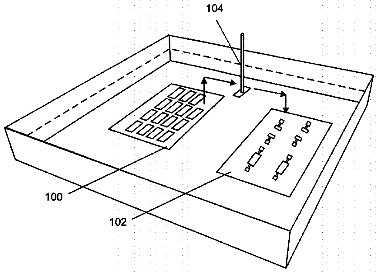
[0044]This disclosure demonstrates the integration of thin-film photonic devices onto a silicon-based host substrate utilizing surface tension-driven FSA and a modified micro-PAP approach. The thin-film format of optical devices allows a topological flat surface after its integration. This leads to a unique advantage: layer-by-layer integration.
[0045]The disclosed integration approach provides exciting opportunities for heterogeneous integration of thin-film devices with high repeatability and improved process yield.
[0046]FIG. 1 shows the disclosed integration approach of thin-film III-V optical devices onto a silicon substrate. Thin-film III-V optical devices are fabricated and transferred onto a temporary carrier 100 (e.g. a glass cover) in water, making them ready for further integration. Also, a silicon host substrate 102 with electrical contacts is prepared and an attracting lubricant medium for self-assembly is selectively formed on their predesigned integration locations. A n...
PUM
| Property | Measurement | Unit |
|---|---|---|
| Thickness | aaaaa | aaaaa |
| Thickness | aaaaa | aaaaa |
| Thickness | aaaaa | aaaaa |
Abstract
Description
Claims
Application Information
 - R&D Engineer
- R&D Manager
- IP Professional
- Industry Leading Data Capabilities
- Powerful AI technology
- Patent DNA Extraction
Browse by: Latest US Patents, China's latest patents, Technical Efficacy Thesaurus, Application Domain, Technology Topic, Popular Technical Reports.
© 2024 PatSnap. All rights reserved.Legal|Privacy policy|Modern Slavery Act Transparency Statement|Sitemap|About US| Contact US: help@patsnap.com