Translucent structure, method for manufacturing same, and article
- Summary
- Abstract
- Description
- Claims
- Application Information
AI Technical Summary
Benefits of technology
Problems solved by technology
Method used
Image

Examples
first embodiment
[0070]FIG. 1 is a schematic sectional view showing a first embodiment of a translucent structure in the present invention. FIG. 2 is a schematic sectional view showing a surface shape of the translucent structure according to the embodiment.
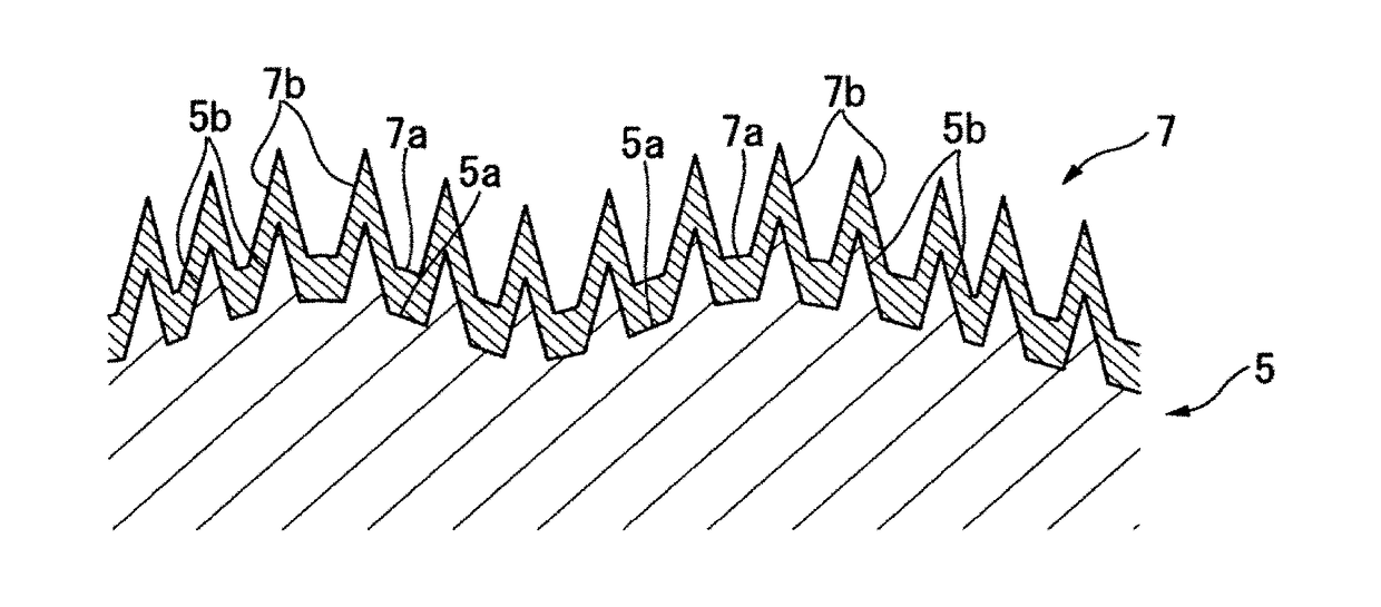
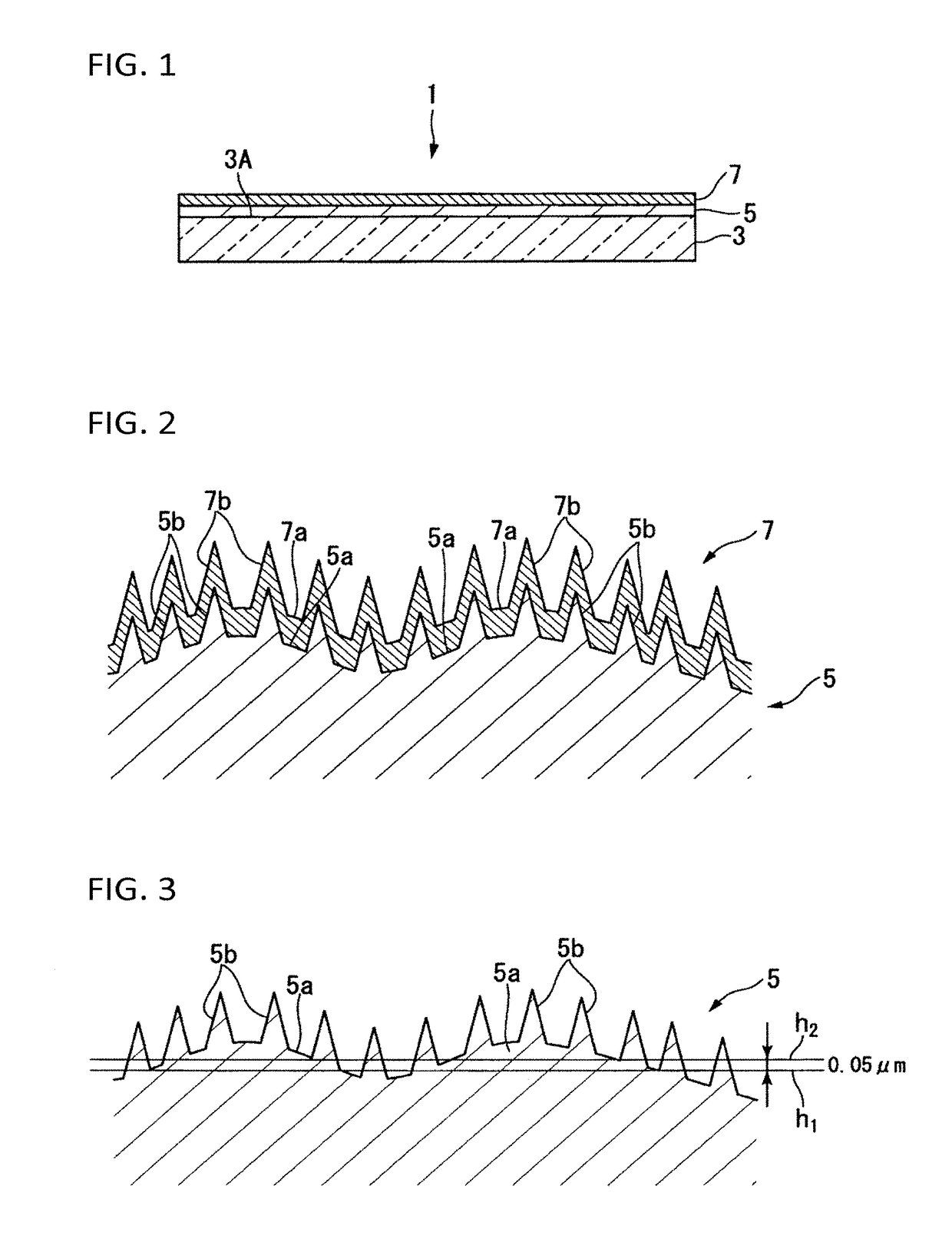
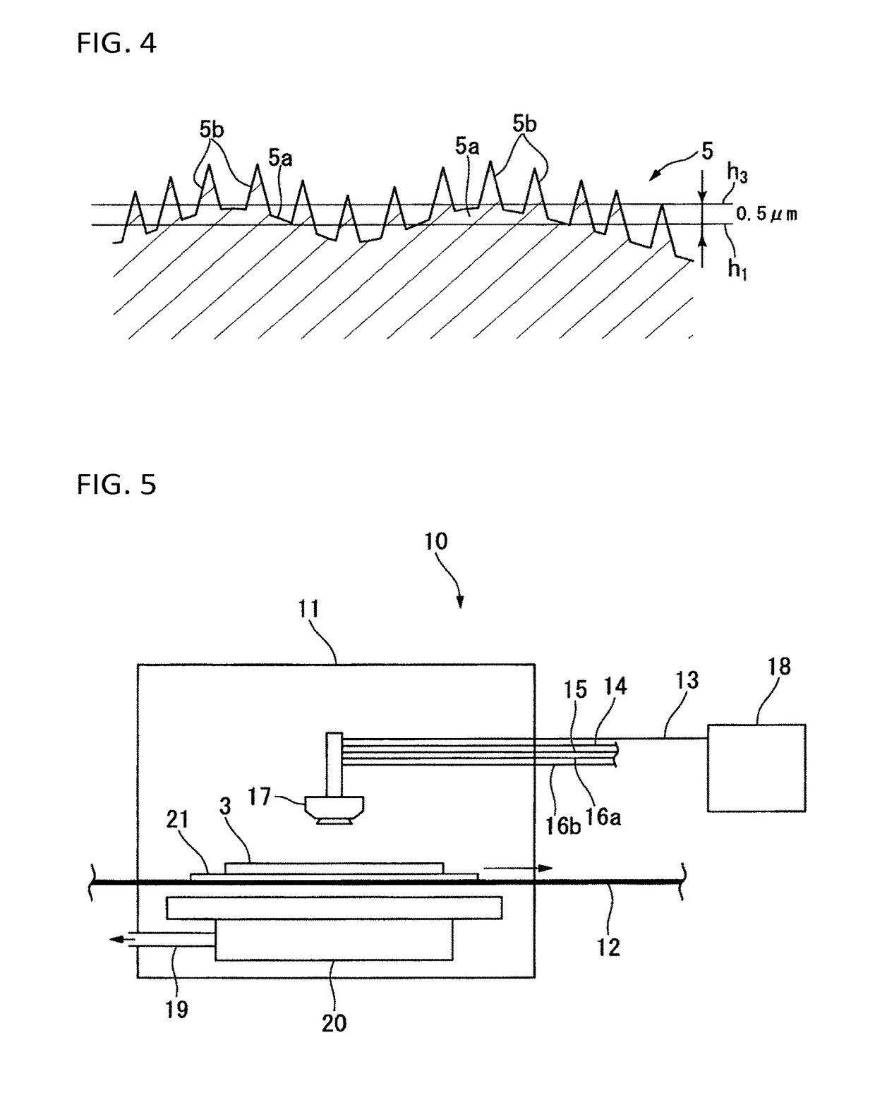
[0071]A translucent structure 1 according to the embodiment has a translucent substrate 3, a base layer 5 formed on a first surface 3A of the translucent substrate 3, and an antireflection layer (hereinafter also referred to as “AR layer”) 7 formed on the base layer 5.
[0072]In the translucent substrate 3, the first surface 3A is located on a visible side. Each of the base layer 5 and the AR layer 7 has a concave and convex structure in its surface. The AR layer 7 is located on the outermost visible side of the translucent structure 1. Therefore, the surface of the AR layer 7 is the visible-side outermost surface of the translucent structure 1.
(Translucent Substrate)
[0073]A substrate which can transmit visible light may be used as the translucent ...
second embodiment
[0339]FIG. 8 is a schematic sectional view showing a second embodiment of a translucent structure in the present invention. FIG. 9 is a schematic sectional view showing a surface shape of the translucent structure according to the second embodiment. In the following embodiment, constituent elements corresponding to those in the aforementioned embodiment will be referenced correspondingly, and detailed description thereof will be omitted.
[0340]A translucent structure 2 according to the embodiment has a translucent substrate 4, and an AR layer 7 formed on a first surface 4A of the translucent substrate 4.
[0341]In the translucent substrate 4, the first surface 4A is located on a visible side. Each of the translucent substrate 4 and the AR layer 7 has a concave and convex structure on its surface. The AR layer 7 is located on the outermost visible side of the translucent structure 2. Therefore, the surface of the AR layer 7 is the visible-side outermost surface of the translucent struct...
third embodiment
[0355]FIG. 10 is a schematic sectional view showing a third embodiment of a translucent structure in the present invention. FIG. 11 is a schematic sectional view showing a surface shape of the translucent structure according to the embodiment.
[0356]A translucent structure 6 according to the embodiment has a translucent substrate 3, a base layer 5 formed on a first surface 3A of the translucent substrate 3, an AR layer 7 formed on the base layer 5, and a water-repellent and oil-repellent layer (hereinafter also referred to as “AFP layer”) 9 formed on the AR layer 7.
[0357]In the translucent substrate 3, the first surface 3A is located on a visible side. Each of the base layer 5, the AR layer 7 and the AFP layer 9 has a concave and convex structure on its surface. In the translucent structure 6, the AFP layer 9 is located on the outermost visible side, and the AR layer 7 is located just under the AFP layer 9. Therefore, the surface of the AFP layer 9 is the visible-side outermost surfa...
PUM
| Property | Measurement | Unit |
|---|---|---|
| Fraction | aaaaa | aaaaa |
| Percent by mass | aaaaa | aaaaa |
| Viscosity | aaaaa | aaaaa |
Abstract
Description
Claims
Application Information