Interconnect circuit methods and devices

a technology of interconnection circuit and circuit mask, applied in the direction of circuit mask, cell component details, cell components, etc., can solve the problem of undesirable proportion

Active Publication Date: 2019-01-17
CELLINK
View PDF0 Cites 5 Cited by
  • Summary
  • Abstract
  • Description
  • Claims
  • Application Information

AI Technical Summary

Benefits of technology

[0004]Provided are interconnect circuits and methods of forming thereof. A method may involve laminating a substrate to a conductive layer followed by patterning the conductive layer. This patterning operation forms individual conductive portions, which may be also referred to as traces or conductive islands. The substrate supports these portions relative to each other during and after patterning. After patterning, an insulator may be laminated to the exposed surface of the pattern...

Problems solved by technology

For example, the third portion may be an...

Method used


Image

  • Interconnect circuit methods and devices
  • Interconnect circuit methods and devices
  • Interconnect circuit methods and devices

Examples


Embodiment Construction

[0031]The ensuing detailed description of embodiments of this disclosure will be better understood when read in conjunction with the appended drawings. As used herein, an element or step recited in the singular and proceeded with the word “a” or “an” should be understood as not excluding plural of said elements or steps, unless such exclusion is explicitly stated. Furthermore, references to “one embodiment” are not intended to be interpreted as excluding the existence of additional embodiments that also incorporate the recited features. Moreover, unless explicitly stated to the contrary, embodiments “comprising” or “having” an element or a plurality of elements having a particular property may include additional elements not having that property.

Introduction

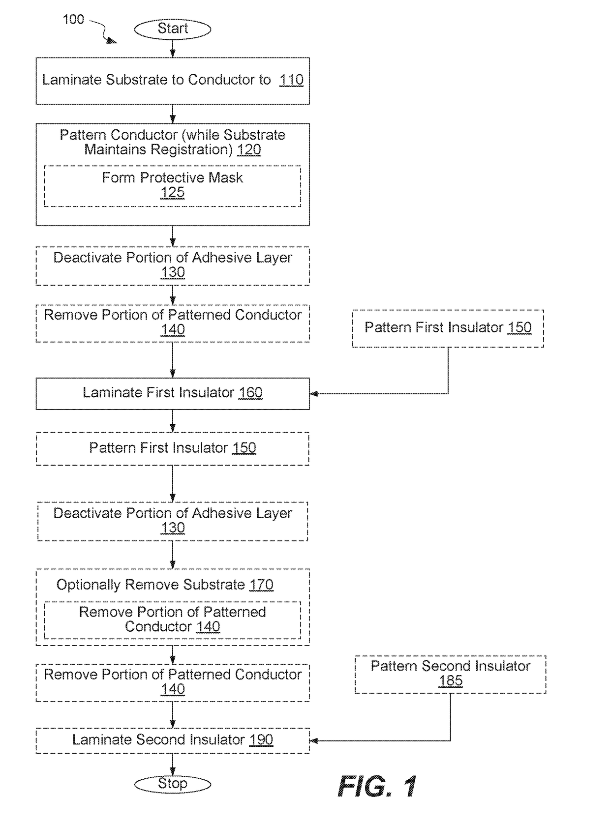
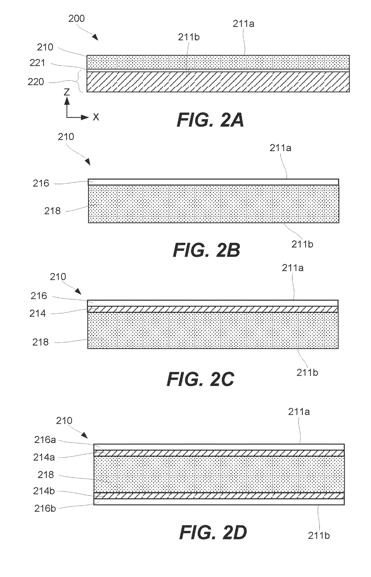
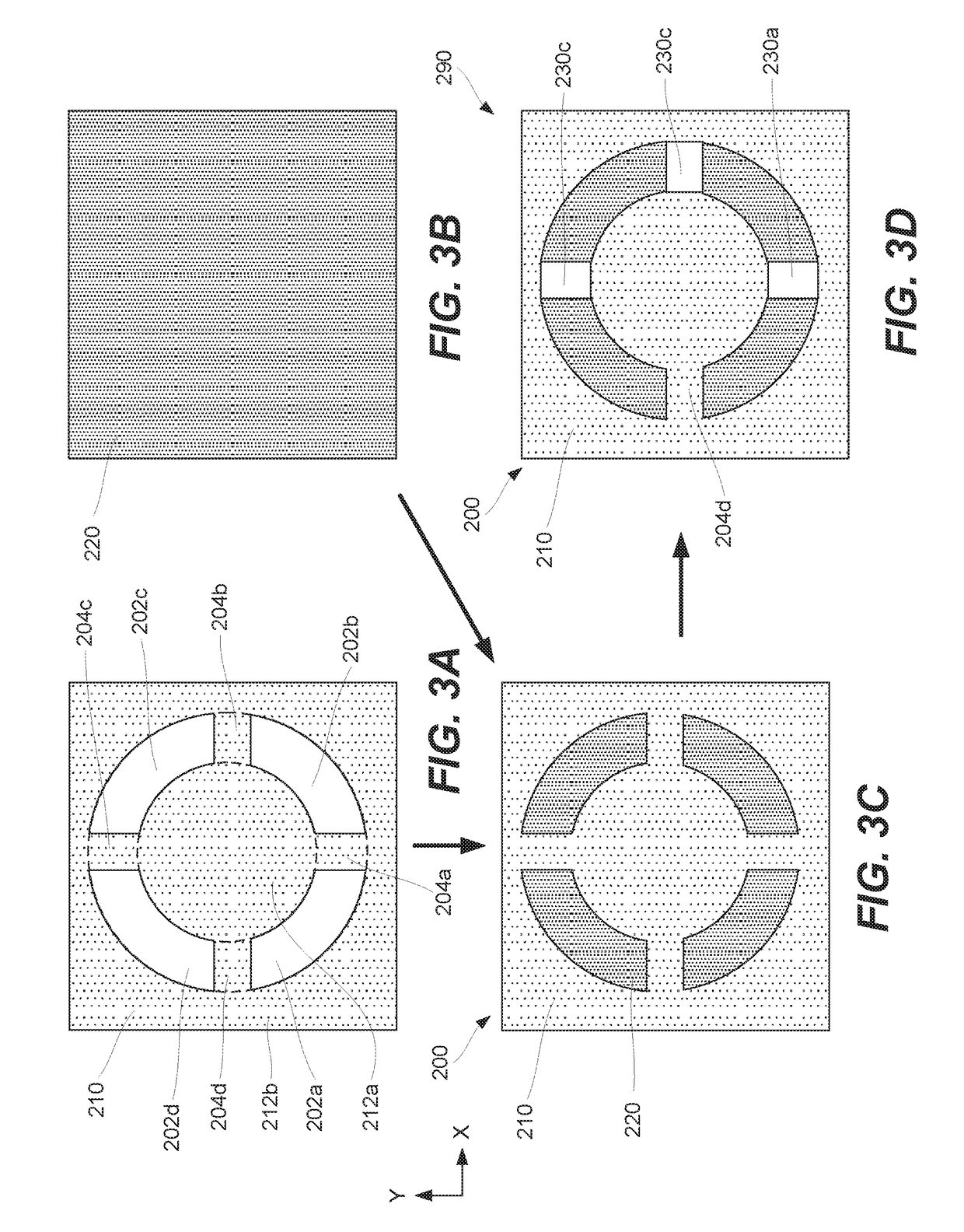
[0032]Interconnect circuits and, more specifically, flexible interconnect circuits described herein, may be used to form electrical connections to various electrical and electronic components and to carry electrical current and / o...


PUM

PropertyMeasurementUnit
Electrical conductoraaaaaaaaaa
Widthaaaaaaaaaa

Abstract

Provided are interconnect circuits and methods of forming thereof. A method may involve laminating a substrate to a conductive layer followed by patterning the conductive layer. This patterning operation forms individual conductive portions, which may be also referred to as traces or conductive islands. The substrate supports these portions relative to each other during and after patterning. After patterning, an insulator may be laminated to the exposed surface of the patterned conductive layer. At this point, the conductive layer portions are also supported by the insulator, and the substrate may optionally be removed, e.g., together with undesirable portions of the conductive layer. Alternatively, the substrate may be retained as a component of the circuit and the undesirable portions of the patterned conductive layer may be removed separately. These approaches allow using new patterning techniques as well as new materials for substrates and/or insulators.

Description

CROSS-REFERENCE TO RELATED APPLICATIONS[0001]This application claims the benefit under 35 U.S.C. § 119(e) of U.S. Provisional Patent Application No. 62 / 531,995, entitled “INTERCONNECT CIRCUIT METHODS AND DEVICES”, filed on Jul. 13, 2017, which is incorporated herein by reference in its entirety for all purposes.BACKGROUND[0002]Electrical interconnects are used for many applications. Some examples of these applications include, but are not limited to, battery packs and solar arrays (interconnecting individual cells), vehicles (connecting different electrical components, e.g., interconnects used as wire harnesses), light fixtures, and many other types of electrical and electronic circuits. While many different kinds of electrical interconnects are currently available, most have limited functionality and are limited to a relatively small set of material choices. For example, a typical printed circuit board (PCB) has a dielectric base with conductive traces formed by chemical etching. D...

Claims


Application Information

Patent Timeline
IPC IPC(8): H05K1/02H05K3/00H01M50/519
CPCH05K3/0073H05K1/0201H05K1/118H05K3/007H05K3/064H05K2201/0145H05K2201/015H05K2201/0154H05K2201/10037Y02E60/10H05K3/20H05K3/046H05K2203/0264H01M50/519H05K3/281H05K3/06H05K3/4623
Inventor COAKLEY, KEVIN MICHAELBROWN, MALCOLM PARKERYANG, DONGAOMILLER, MICHAEL LAWRENCELEGO, PAUL HENRY
Owner CELLINK
Why Eureka
Try Eureka