
Semiconductor package and manufacturing method thereof

Active Publication Date: 2019-05-02
SAMSUNG ELECTRO MECHANICS CO LTD
View PDF0 Cites 5 Cited by
  • Summary
  • Abstract
  • Description
  • Claims
  • Application Information

AI Technical Summary

Benefits of technology

This patent describes a semiconductor package that includes an antenna unit on top of a lower package that contains electronic devices. The antenna unit has a ground portion, a radiating portion with radiators, and a support portion separating the radiating portion and the ground portion. The support portion may have a first and second support portion, with the second support portion supporting a radiator. The lower package may have a substrate and rewiring layers, with the ground portion disposed on the substrate. The semiconductor package also includes a connecting conductor that electrically connects the antenna unit and the substrate. The antenna unit can transmit and receive radio signals in ultra high frequency or millimeter wavelength bands. The technical effects of this patent include improved radio signal transmission and reception in semiconductor packages.

Problems solved by technology

In the millimeter wave band, a wavelength of a frequency is shortened to millimeter units, and thus, the use of conventional semiconductor package structures may degrade performance.

Method used


Image

  • Semiconductor package and manufacturing method thereof
  • Semiconductor package and manufacturing method thereof
  • Semiconductor package and manufacturing method thereof

Examples


Embodiment Construction

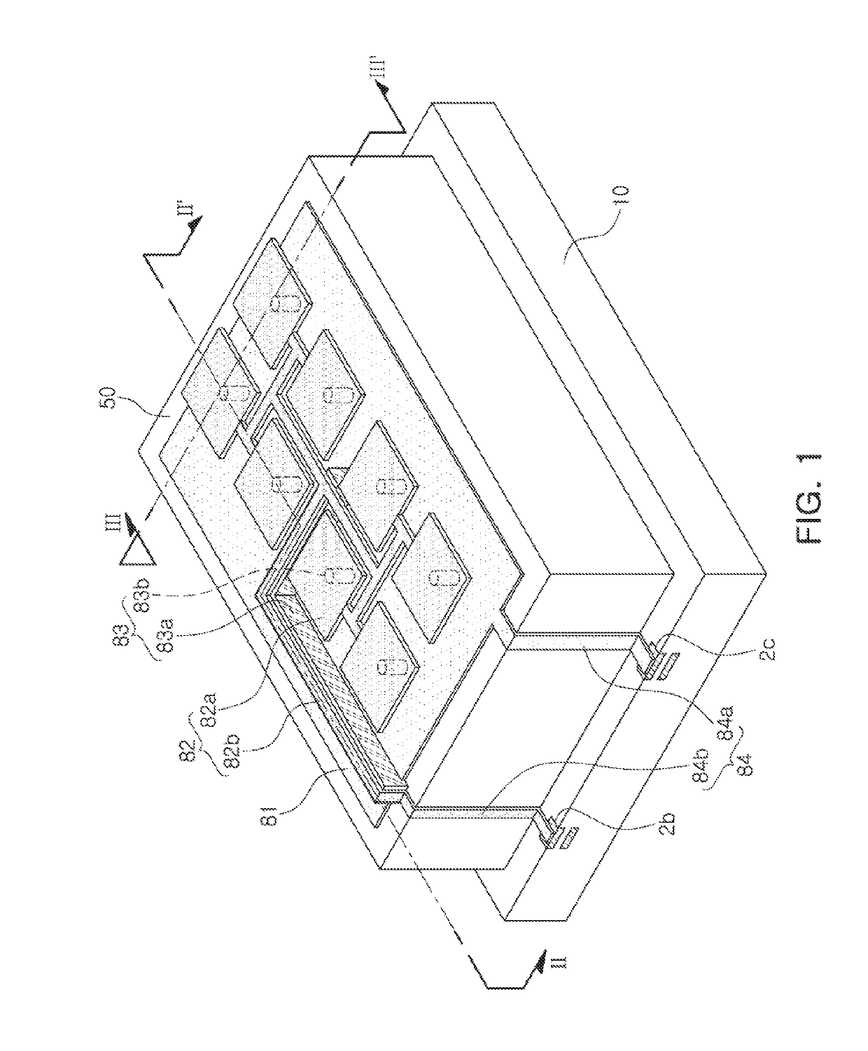
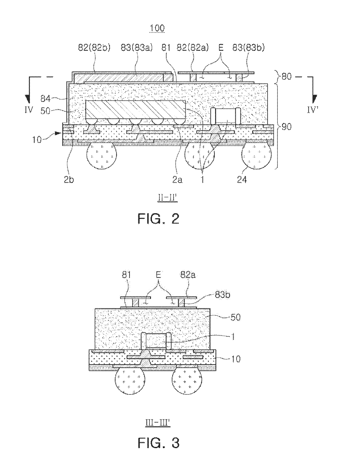
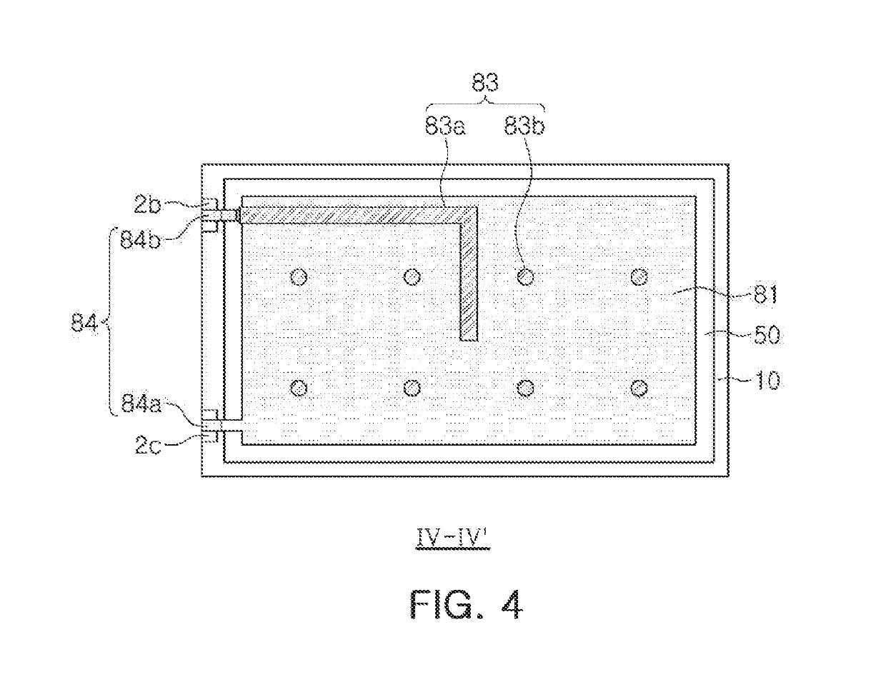
[0036]The following detailed description is provided to assist the reader in gaining a comprehensive understanding of the methods, apparatuses, and / or systems described herein. However, various changes, modifications, and equivalents of the methods, apparatuses, and / or systems described herein will be apparent after an understanding of the disclosure of this application. For example, the sequences of operations described herein are merely examples, and are not limited to those set forth herein, but may be changed as will be apparent after an understanding of the disclosure of this application, with the exception of operations necessarily occurring in a certain order. Also, descriptions of features that are known in the art may be omitted for increased clarity and conciseness.

[0037]The features described herein may be embodied in different forms, and are not to be construed as being limited to the examples described herein. Rather, the examples described herein have been provided mer...


PUM


Abstract

A semiconductor package includes a lower package including at least one electronic device, and an antenna unit disposed on an upper surface of the lower package, wherein the antenna unit includes: a ground portion disposed on an upper surface of the lower package, a radiating portion disposed to be spaced apart from the ground portion, and a support portion separating the radiating portion and the ground portion, and at least a portion between the radiating portion and the grounding portion is empty space.

Description

CROSS-REFERENCE TO RELATED APPLICATION[0001]This application claims the benefit under 35 USC § 119(a) of Korean Patent Application No. 10-2017-0145398 filed on Nov. 2, 2017 in the Korean Intellectual Property Office, the entire disclosure of which is incorporated herein by reference for all purposes.BACKGROUNDField[0002]The disclosure relates to a semiconductor package and a manufacturing method thereof.Description of Related Art[0003]In order to use high-quality and high-capacity data at a high speed, frequency bands of semiconductor packages have increased. For example, for semiconductor packages for wireless communications, a technique using a millimeter wave band of 27 GHz or higher is considered.[0004]In the millimeter wave band, a wavelength of a frequency is shortened to millimeter units, and thus, the use of conventional semiconductor package structures may degrade performance.SUMMARY[0005]This Summary is provided to introduce a selection of concepts in a simplified form tha...

Claims


Application Information

Patent Timeline
IPC IPC(8): H01Q1/22H01Q1/44H01Q1/40H01L23/552H01L23/538H01L23/66H01L23/31H01L23/00G06K19/077
CPCH01Q1/2283H01Q1/44H01Q1/40H01L23/552H01L23/5383H01L23/66H01L23/3128H01L24/97G06K19/07749H01L2223/6677H01L2224/16227H01L2224/97H01L2924/15311H01L2924/19105H01Q1/48H01Q9/0407H01Q9/045H01Q21/0075H01Q21/0087H01Q21/065H01Q21/30H01L21/561H01L21/6835H01L2221/68345H01L2221/68359H01L2224/16237H01L2224/16235H01L23/49816H01L23/49822H01L23/5389H01L2224/81H01L23/52H01L24/27H01L24/28H01L23/28H01L23/49827
Inventor PARK, SEUNG WOOKPARK, TAH JOONJUNG, JAE HYUNLEE, HWA SUNNA, SEONG HUN
Owner SAMSUNG ELECTRO MECHANICS CO LTD
Learn More