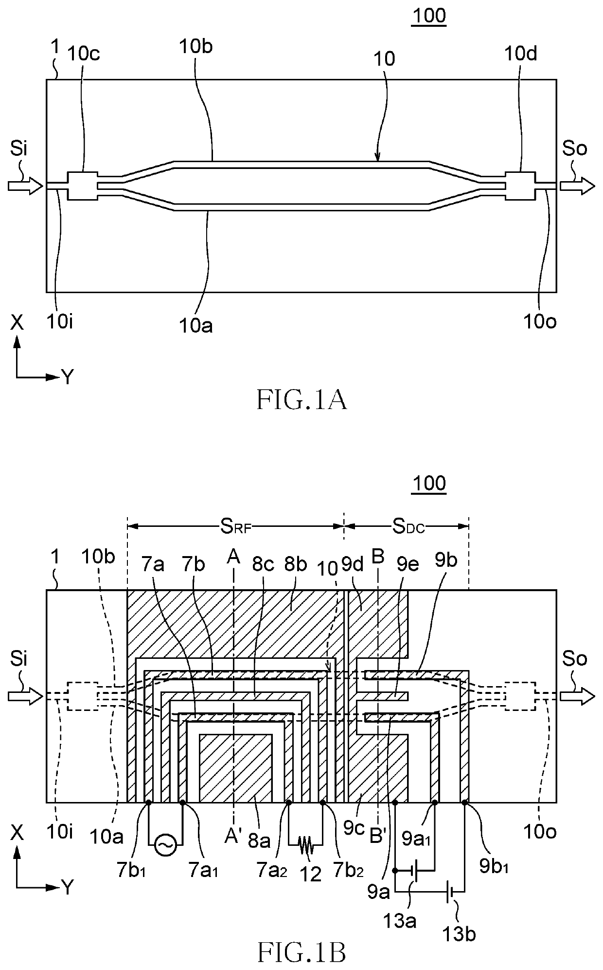
Optical modulator

a modulator and optical technology, applied in the field of optical modulators, can solve the problems of limiting the length of high-speed modulation, and the entire length of the modulator is as long as about 10 cm, and achieve the effect of reducing dc drift and stabilizing the structure over a long period of tim

Active Publication Date: 2020-10-01
TDK CORPARATION
View PDF0 Cites 0 Cited by
  • Summary
  • Abstract
  • Description
  • Claims
  • Application Information

AI Technical Summary

Benefits of technology

[0032]According to the present invention, there can be provided an optical modulator having a device structure stably controllable over a long period of time by reducing the DC drift.

Problems solved by technology

The direct modulation system does not require the optical modulator and is thus low in cost, but has a limitation in terms of high-speed modulation and, thus, the external modulation system is used for high-speed and long-distance applications.
Although high-speed optical modulators having a modulation speed of 40 Gb / s or higher are commercially available, they have a major drawback that the entire length thereof is as long as about 10 cm.

Method used


Image

  • Optical modulator
  • Optical modulator
  • Optical modulator

Examples


examples

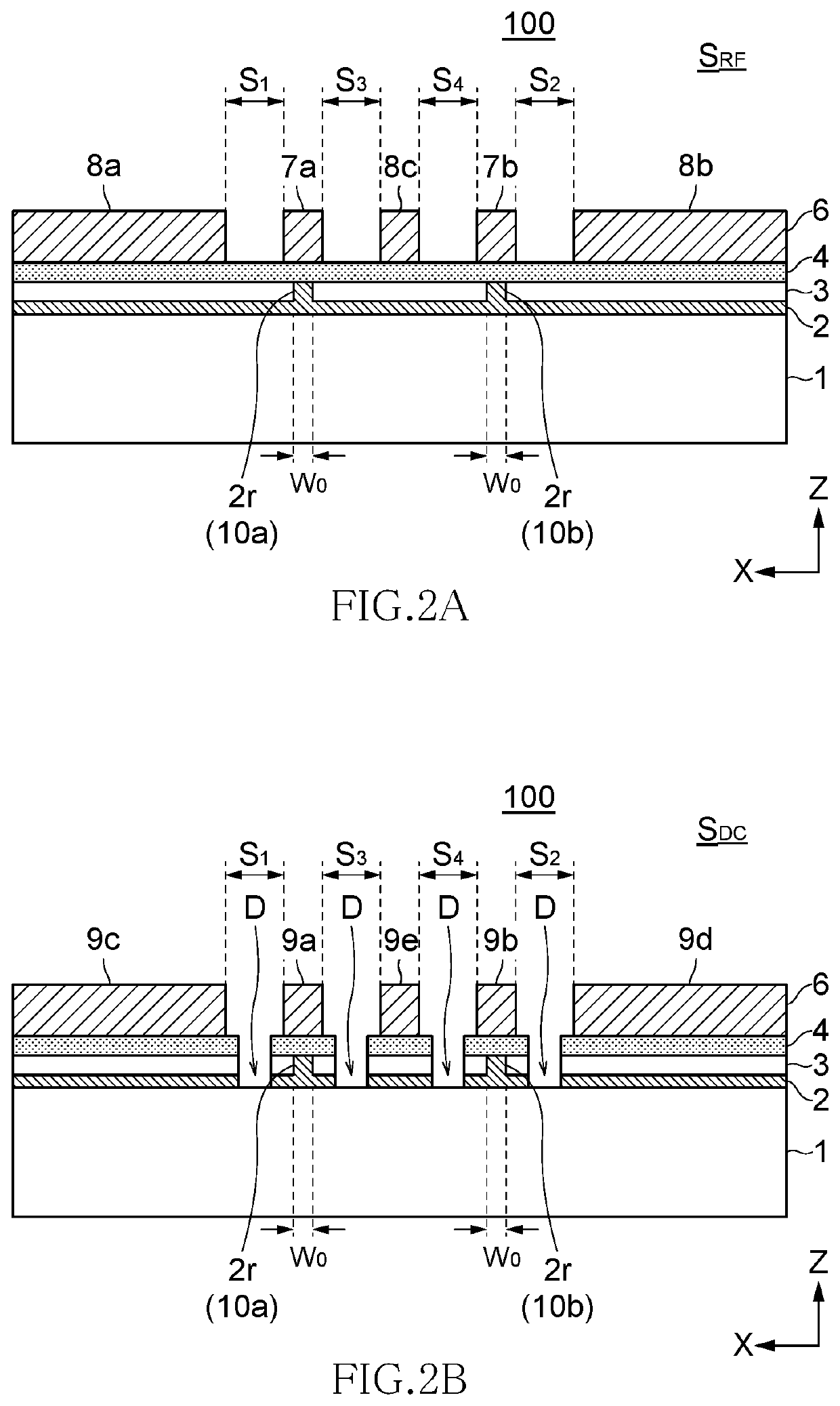
[0118]An acceleration test as to the DC drift was carried out for the optical modulators according to Comparative Examples and Examples. In this acceleration test, a change in drift amount Vdrift / Vbias when a DC bias Vbias was continued to be applied for 24 hours under a high temperature of 140° C. was determined.

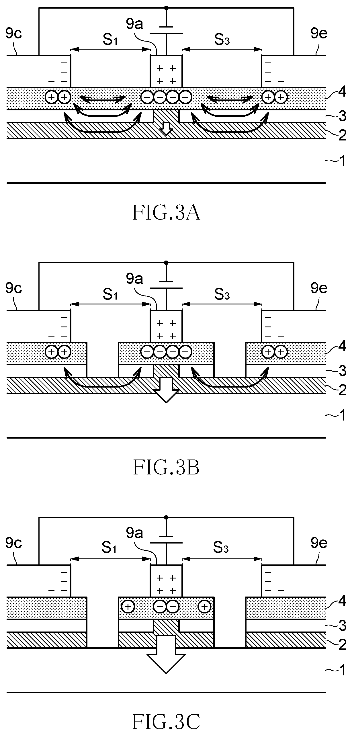
[0119]Optical modulators according to Comparative Examples 1A and 1B each have the cross-sectional structure of FIG. 3A, that is, they each have a conventional structure in which the waveguide layer and buffer layer are formed over the entire surface. The buffer layer of Comparative Example 1A is formed of an oxide La—Al—O (composition A) containing La and Al as main components, and the buffer layer of Comparative Example 1B is formed of an oxide Si—In—O (composition B) containing Si and In as main components.

[0120]Optical modulators according to Comparative Examples 2A and 2B each have the cross-sectional structure of FIG. 3B, that is, they each have a conventional structu...


PUM

PropertyMeasurementUnit
thicknessaaaaaaaaaa
lengthaaaaaaaaaa
widthaaaaaaaaaa

Abstract

An optical modulator includes: a substrate; a waveguide layer including first and second optical waveguides formed of an electro-optic material film on the substrate to have a ridge shape and to be disposed adjacent to each other; an RF part that applies a modulated signal to the optical waveguides; and a DC part that applies a DC bias to the optical waveguides. The DC part includes: a buffer layer covering at least upper surfaces of the optical waveguides; a first bias electrode opposed to the first optical waveguide through the buffer layer; and a second bias electrode provided adjacent to the first bias electrode. A first DC bias voltage is applied between the first and second bias electrodes. A waveguide layer removal area in which at least part of the waveguide layer is removed is provided at least under an area between the first and second bias electrodes.

Description

TECHNICAL FIELD[0001]The present invention relates to an optical modulator used in the fields of optical communication and optical measurement and, more particularly, to an electrode structure of a Mach-Zehnder optical modulator.BACKGROUND ART[0002]Communication traffic has been remarkably increased with widespread Internet use, and optical fiber communication is becoming significantly important. The optical fiber communication is a technology that converts an electric signal into an optical signal and transmits the optical signal through an optical fiber and has wide bandwidth, low loss, and resistance to noise.[0003]As a system for converting an electric signal into an optical signal, there are known a direct modulation system using a semiconductor laser and an external modulation system using an optical modulator. The direct modulation system does not require the optical modulator and is thus low in cost, but has a limitation in terms of high-speed modulation and, thus, the exter...

Claims


Application Information

Patent Timeline
Patent Type & Authority Applications(United States)
IPC IPC(8): G02F1/035
CPCG02F1/035G02F1/011G02F2201/063G02F1/2255G02F2202/20G02F2203/20G02F2201/127G02B2006/12142G02F1/212G02F2203/21
Inventor IWATSUKA, SHINJIENDO, MAKOTOSASAKI, KENJI
Owner TDK CORPARATION
Why Eureka
Try Eureka