

Array substrate and manufacturing method thereof, and display panel
- Summary
- Abstract
- Description
- Claims
- Application Information
AI Technical Summary
Benefits of technology
Problems solved by technology
Method used
Image

Examples
Embodiment Construction
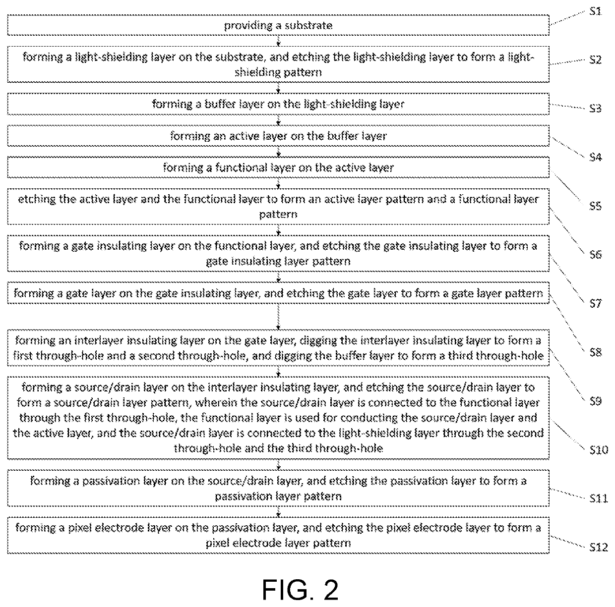
[0032]The present disclosure provides an array substrate and a manufacturing method thereof, and a display panel. In order to make purposes, technical solutions, and effects of the present disclosure clearer and more definite, the following further describes the present disclosure in detail with reference to the drawings and embodiments. It should be understood that the specific embodiments described herein are only used to explain the present disclosure, and are not intended to limit the present disclosure.
[0033]Embodiments of the present disclosure are directed to the technical problems that the current display panel damages the active layer during the preparation process, which causes the performance of thin film transistors to decrease, and the embodiments of the present disclosure are used for solving the technical problems.
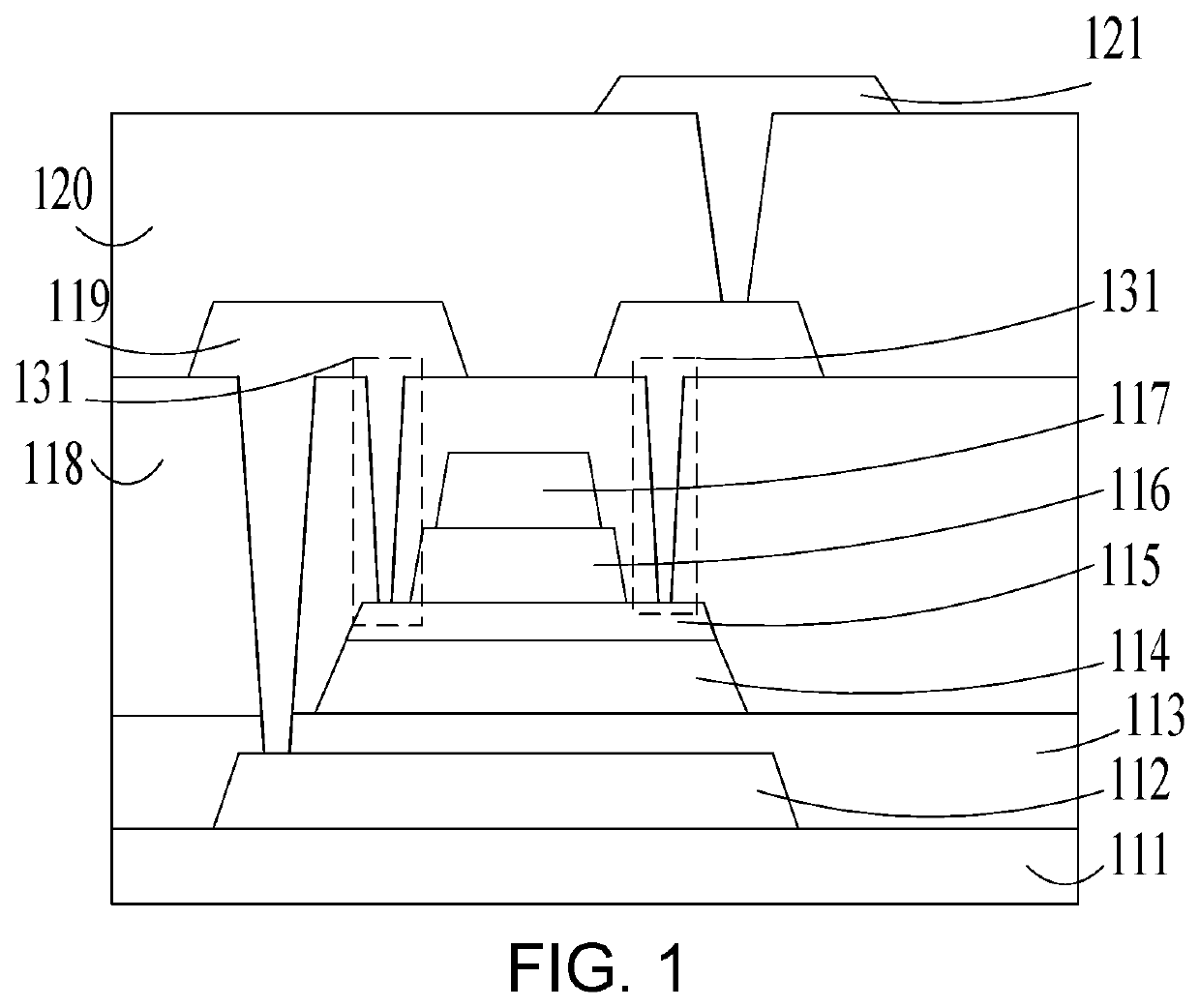
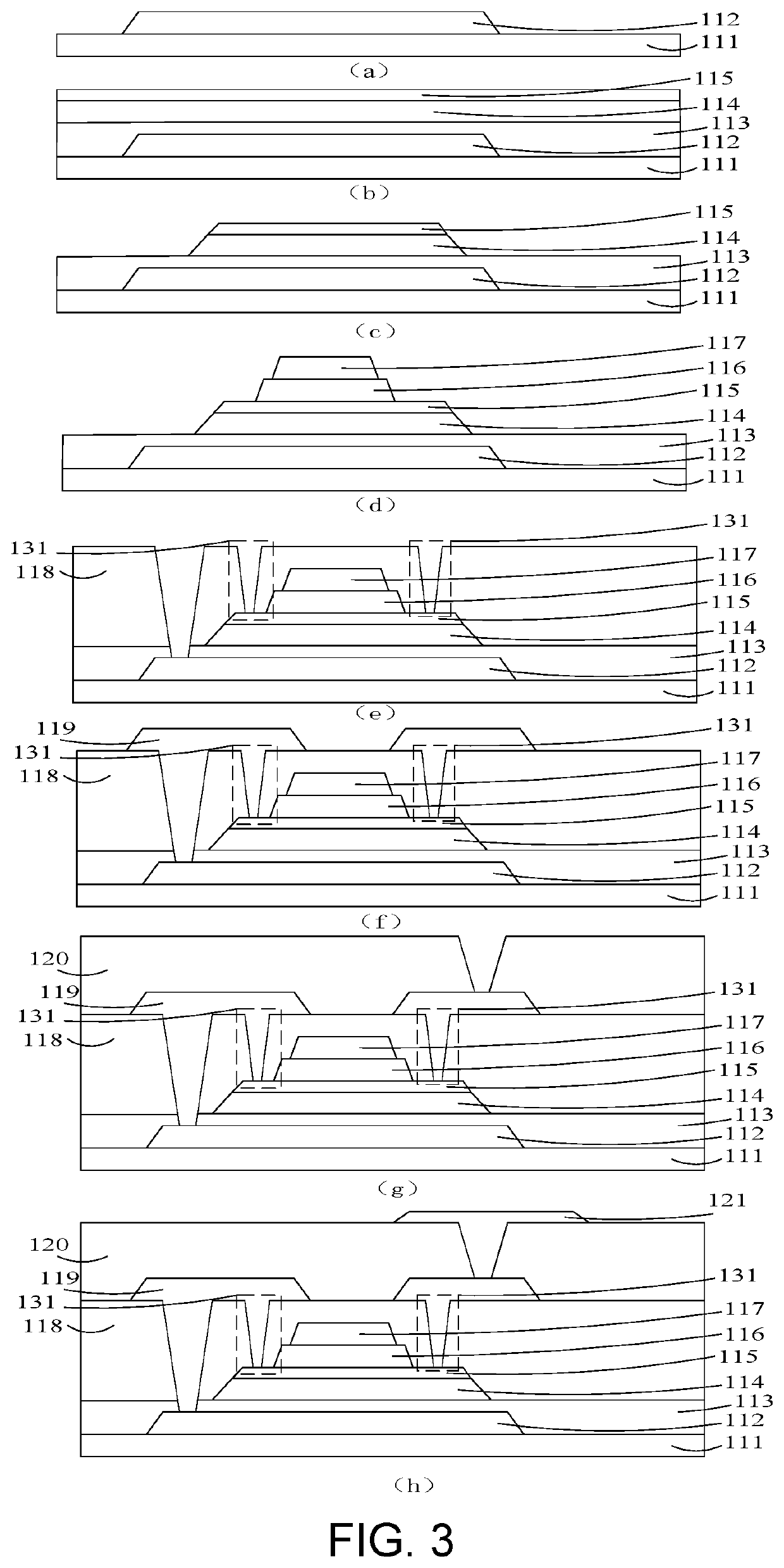
[0034]As shown in FIG. 1, an embodiment of the present disclosure provides an array substrate. The array substrate comprises a substrate 111, a buffer layer...
PUM
 Abstract
Description
Claims
Application Information