Supercharge Your Innovation With Domain-Expert AI Agents!

Electronic device assembly

a technology of electronic devices and components, applied in the direction of coupling device connections, instruments, details of portable computers, etc., can solve problems such as privacy leakag

Active Publication Date: 2022-07-28
ACER INC
View PDF21 Cites 0 Cited by
  • Summary
  • Abstract
  • Description
  • Claims
  • Application Information

AI Technical Summary

Benefits of technology

The patent describes an electronic device assembly where a detachable lens module can be easily attached and detached from an electronic device body. This allows the lens module to be used as needed, and when not in use, it can be stored safely by connecting the lens module to the electronic device body using a joining unit. The housing of the electronic device body can have openings or a recess to accommodate the lens module. The technical effect of this invention is to provide a more flexible and convenient electronic device assembly with the ability to customize the lens module for different needs and to protect the lens when not in use.

Problems solved by technology

However, there are fears that the lens fixed above the display screen may cause privacy leakage.

Method used


Image

  • Electronic device assembly
  • Electronic device assembly
  • Electronic device assembly

Examples


Embodiment Construction

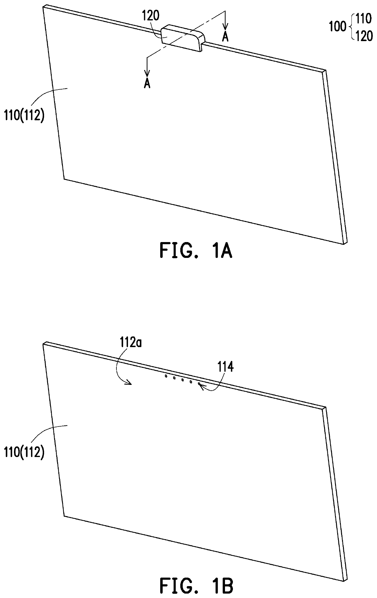
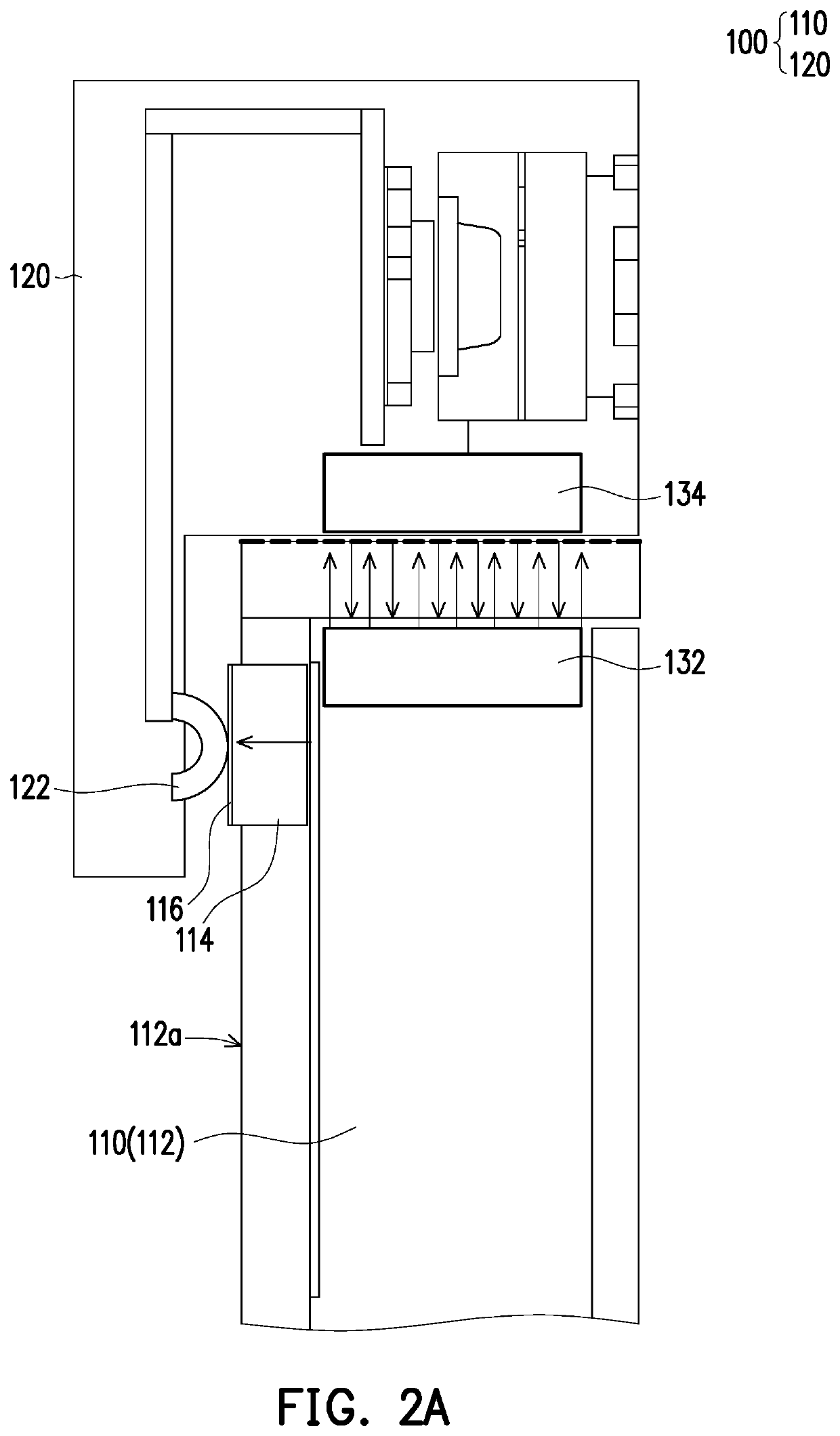
[0025]FIG. 1A is a schematic view of an electronic device assembly, and FIG. 1B is a schematic view of an electronic device body. An electronic device assembly 100 includes an electronic device body 110 and a detachable lens module 120. Referring to FIG. 1A and FIG. 1B together, the electronic device body 110 may be a notebook computer or a tablet computer and has a housing 112 and a first joining unit 114, wherein the first joining unit 114 is disposed on the housing 112.

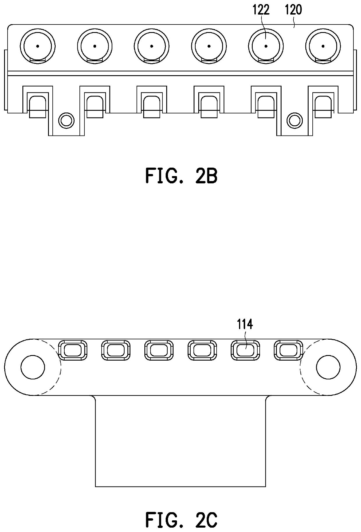
[0026]In the present embodiment, the first joining unit 114 may be a plurality of pads exposed from a surface (back surface) 112a of the housing 112. Moreover, to make the housing 112 of the electronic device body 110 appear uniform in color, an electroplating layer 116 may further be formed on the pads, and the electroplating layer 116 is of the same color as the housing 112.

[0027]The detachable lens module 120 is detachably assembled onto the housing 112, wherein the detachable lens module 120 may be assembled on...


PUM


Abstract

An electronic device assembly is provided, including an electronic device body and a detachable lens module. The electronic device body has a housing and a first joining unit, wherein the first joining unit is disposed on the housing. The detachable lens module is detachably assembled onto the housing and has a second joining unit, wherein the first joining unit is joined to the second joining unit to electrically connect the detachable lens module to the electronic device body.

Description

CROSS-REFERENCE TO RELATED APPLICATION[0001]This application is a divisional application of and claims the priority benefit of U.S. application Ser. No. 16 / 905,922, filed on Jun. 19, 2020, which claims the priority benefit of Taiwan application serial no. 109200733, filed on Jan. 17, 2020. The entirety of each of the above-mentioned patent applications is hereby incorporated by reference herein and made a part of this specification.BACKGROUNDTechnical Field[0002]The disclosure relates to a device assembly, and more particularly, to an electronic device assembly.Related Art[0003]In order to maximize a screen-to-body ratio of electronic devices, slim border design has become a trend in recent years. Thus, the space above a display screen, which was reserved for placing a lens, has to be sacrificed.[0004]The border is used to hide wires therein and provide enough space for the lens. However, there are fears that the lens fixed above the display screen may cause privacy leakage.SUMMARY[...

Claims


Application Information

Patent Timeline
Patent Type & Authority Applications(United States)
IPC IPC(8): G06F1/16
CPCG06F1/1632H01R13/26G06F1/1616G06F1/1656G06F1/1607G06F1/1626G06F1/1686H01R13/24H01R13/6205
Inventor WANG, YU-SHIHHUANG, YI-TALIU, CHIH-CHUNLING, CHENG-NANTAI, WEN-CHIEHLAI, CHI-HUNGLEE, WU-CHENLIN, PIN-CHUEHLIAO, CHIH-WEIPAI, TING-WENCHEN, WEN-CHIEH
Owner ACER INC
Features
  • R&D
  • Intellectual Property
  • Life Sciences
  • Materials
  • Tech Scout
  • Unparalleled Data Quality
  • Higher Quality Content
  • 60% Fewer Hallucinations
Learn More