Display panel and display device using the same

a display panel and display device technology, applied in the field of liquid crystal display panels, can solve the problems of image prone to be displayed at a low luminance, image distortion, light leakage,

Inactive Publication Date: 2001-04-17
GK BRIDGE 1
View PDF28 Cites 109 Cited by
  • Summary
  • Abstract
  • Description
  • Claims
  • Application Information

AI Technical Summary

Problems solved by technology

However, the liquid crystal display panel has difficulty in securing a relatively large display format and, therefore, a compromise has been made to incorporate the liquid crystal panel in a projection type display device of a type employing an optical system for projecting images generated by the liquid crystal panel onto a screen.
Passage of light through the display region of the TN liquid crystal display panel suffices, and light transmitted from somewhere other than the display region of the TN liquid crystal display panel is of no use and may constitute a cause of darkening of images being displayed.
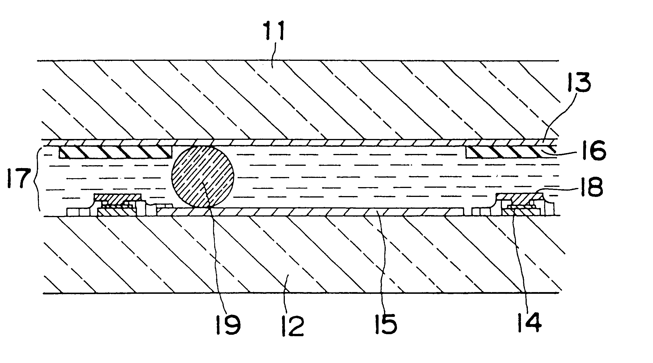
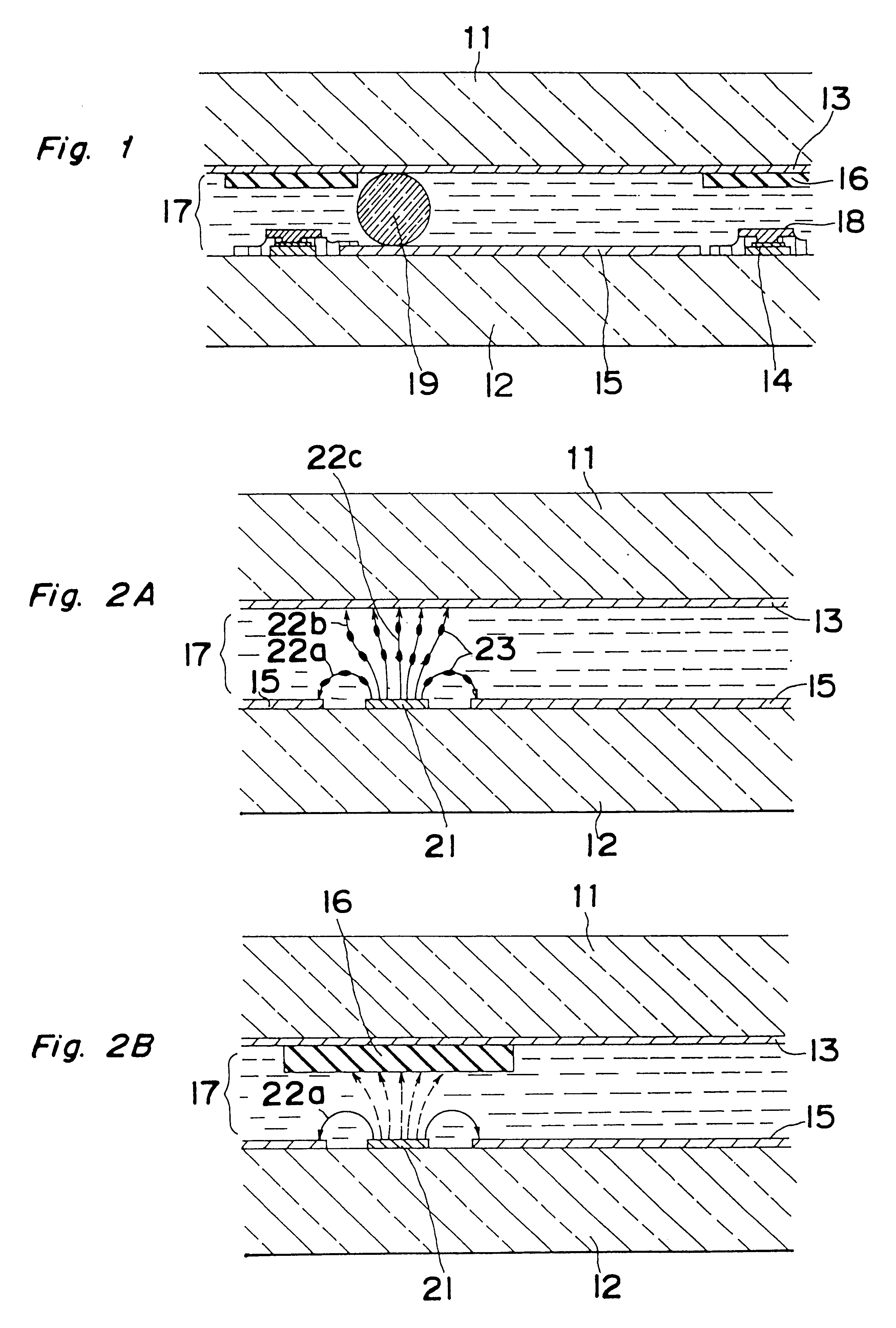
Also, any error in fitting the TN liquid crystal display panel to the chassis through the printed circuit board may result in leakage of light from one end while the opposite end will shield a portion of the display region of the display panel.
This means that only about 25% of the total light incident upon the TN liquid crystal display panel is utilized effectively and, accordingly, the TN liquid crystal display panel has a problem in that images are apt to be displayed at a low luminance.
The use of the rubbing process results in increase of the number of manufacturing steps which in turn brings about increase in manufacturing cost.
Reduction in pixel size in turn brings about an increased number of surface irregularities per unit area resulting from signal lines, thin-film transistors and other elements.
The presence of the increased surface irregularities obviously hampers a satisfactory rubbing.
While the display panel useable in the NW mode is considered excellent in respect of color reproducibility of images being displayed, it has a problem in that light tends to leak from around each pixel.
However, this is not an effective method since the increased width of the black matrix 381 results in reduction in the area of closure of the pixels which in turn brings about reduction in luminance of the images being displayed.
Accordingly, the efficiency of utilization of light is low and the display luminance is low.
Moreover, light impinging upon the black matrix does in turn heat the display panel to an elevated temperature which subsequently brings about reduction in lifetime of the display panel as a whole.
Similarly, the projection type display device in which the TN liquid crystal display panel is used as a light valve has a low efficiency of utilization of light, accompanied by reduction in luminance of the images being projected onto the screen.
Portion of the UV-curable resin which has been radiated by ultraviolet rays of light is cured to result in phase separation between the resin component and the liquid crystal component, but the remaining portion of the UV-curable resin which has not been radiated remains uncured.
The presence of that portion of the UV-curable resin which has been left uncured adversely affects the reliability and the lifetime of the PD liquid crystal display panel.
The presence of the black matrix 381 makes it difficult to fix UV radiating conditions during the manufacture of the display panel.
As hereinabove discussed, if the black matrix 381 is formed, even the slightest change in temperature during the manufacture and the intensity of UV radiation bring about a considerable change in average particle size of the liquid crystal material overlaying the pixel electrodes or in average pore size of the polymer network overlaying the pixel electrodes, thereby imposing limitations on the manufacturing condition.
Accordingly, it is difficult to manufacture constantly the polymer dispersed liquid crystal display panels having an equal operating characteristic.
Where the polymer dispersed liquid crystal display panel is used as a light valve in the projection type display device, the presence of that portion of the UV-curable resin which has been left uncured in the display panel tends to constitute a cause of considerable deterioration in performance of the polymer dispersed liquid crystal display panel.
This appears to result from the fact that, in the projection type display device, light of an intensity of about some ten thousand luxes or higher falls on the display panel, subjecting the latter to light-induced and heat-induced stresses.
As hereinbefore discussed, in the prior art TN liquid crystal display panel, the efficiency of utilization of light is relatively low because of the use of the polarizing plate, making it impossible to accomplish a high luminance display.
Also, though the high luminance display can be attained with the polymer dispersed liquid crystal display panel, the prior art structure is instable because of that portion of the UV-curable resin remaining uncured and cannot be employed in practice.
Also, the manufacturing tolerance thereof is extremely limited, making it difficult to obtain constantly the polymer dispersed liquid crystal display panel having a high light scattering characteristic.
As hereinbefore discussed, the TN liquid crystal display panel requires the use of the polarizing plate to accomplish light modulation and is ineffective to accomplish a high luminance display because of a relatively low efficiency of unitization of light.
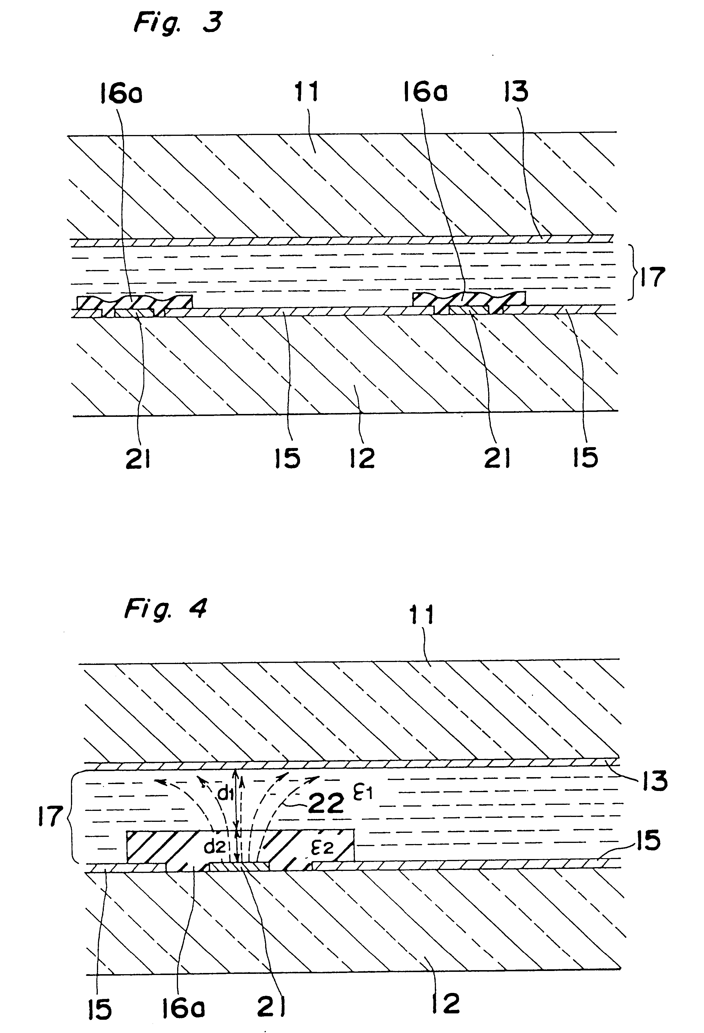
However, the display panel in which the polymer dispersed liquid crystal material is employed as a light modulating layer has some problems in that the retentivity is low, light leakage is apt to occur from around the pixel electrodes and secondary light scattering tends to result from scattering of light in the liquid crystal layer.
All of these problems are peculiar to a display device which utilizes as a light valve a display panel which is effective to modulate light as a function of change in light scattering.

Method used


Image

  • Display panel and display device using the same
  • Display panel and display device using the same
  • Display panel and display device using the same

Examples


Embodiment Construction

The display panel according to a first aspect of the present invention is utilized as incorporated in a touch panel as shown in FIG. 23. The display device can be applied in a system in which, when a sensor 236 is depressed with the aid of a pen or a key, a voltage is applied to a light modulating layer 17 of the display panel so that alphanumeric characters can be displayed through the display panel or the like.

The display panel includes a first electrode substrate 214 formed with first electrodes 216, a second electrode substrate 215 formed with second electrodes 217, and a light modulating layer 17 sandwiched between the first and second electrode substrates 214 and 215 for modulating light as a function of change in light scattering. At least one of the first and second electrode substrates 214 and 215 has a multi-layered dielectric film 212 formed thereon in a predetermined pattern.

Preferably, the second electrodes 217 may be reflective electrodes formed with light reflecting f...


PUM


Abstract

A liquid crystal display panel includes a counter substrate having a counter electrode and a multi-layered dielectric film both formed thereon, and an array substrate formed with pixel electrodes and thin-film transistors serving as switching elements. A layer of polymer dispersed liquid crystal material containing a UV-curable resin component and a liquid crystal component is sandwiched and sealed between the counter and array substrates. A light shielding film is formed over each thin-film transistor. The multi-layered dielectric film is a laminated structure of alternating thin-films of SiO2 and HfO2. Since the multi-layered dielectric film is of a nature capable of transmitting UV-rays of light therethrough, the UV-curable resin component positioned underneath the multi-layered dielectric film can be cured during the manufacture. Also, since the multi-layered dielectric film is of a nature capable of reflecting light of a visible region, it serves as a black matrix, reflecting the visible light modulated by the display panel. Black beads are used to keep the film thickness of the liquid crystal layer at a predetermined value. Preferably, a dielectric thin-film having a relative dielectric constant smaller than that of the liquid crystal material is formed on signal lines for transmitting signals to the thin-film transistors, to thereby accomplish an electromagnetic shield. Where color filters are to be formed on the pixel electrodes, those color filters may be formed on the signal lines to accomplish the electromagnetic shield.

Description

1. (Field of the Invention)The present invention relates to a liquid crystal display panel utilizable as a touch panel or for the display of televised images, a projection type display device utilizing the liquid crystal display panel as a light valve for the display of images in the form as projected onto a screen, and a viewfinder utilizing the liquid crystal display panel as a display monitor for monitoring images being videoed.2. (Description of the Prior Art)The liquid crystal display panel is known to be light-weight and thin in thickness as compared with a cathode ray tube and a variety of liquid crystal display panels have been developed. Recent application of the liquid crystal panel is a display unit in pocketable television receiver sets and a display unit in viewfinders of video cameras. However, the liquid crystal display panel has difficulty in securing a relatively large display format and, therefore, a compromise has been made to incorporate the liquid crystal panel ...

Claims


Application Information

Patent Timeline
Patent Type & Authority Patents(United States)
IPC IPC(8): G02F1/13G02F1/1335G02F1/1333G02F1/1334H04N9/31G02F1/1339G03B21/10G03B21/14
CPCG02F1/133345G02F1/1334G02F1/133512G02F1/133526G03B21/10G03B21/14H04N9/3105H04N9/3197G02F1/133502G02F1/13394G02F2203/02G02F2203/055G03B21/006
Inventor TAKAHARA, HIROSHISANNOHE, SHINYA
Owner GK BRIDGE 1
Why Eureka
Try Eureka