Color shifting thin film pigments
a thin film pigment and color shifting technology, applied in the field of color shifting thin film pigments, can solve the problems of mechanical stress in the large number of layers used in all-dielectric stacks, and achieve the effects of easy and economical utilization, high chroma, and wide range of color shifting properties
- Summary
- Abstract
- Description
- Claims
- Application Information
AI Technical Summary
Benefits of technology
Problems solved by technology
Method used
Image
Examples
example 1
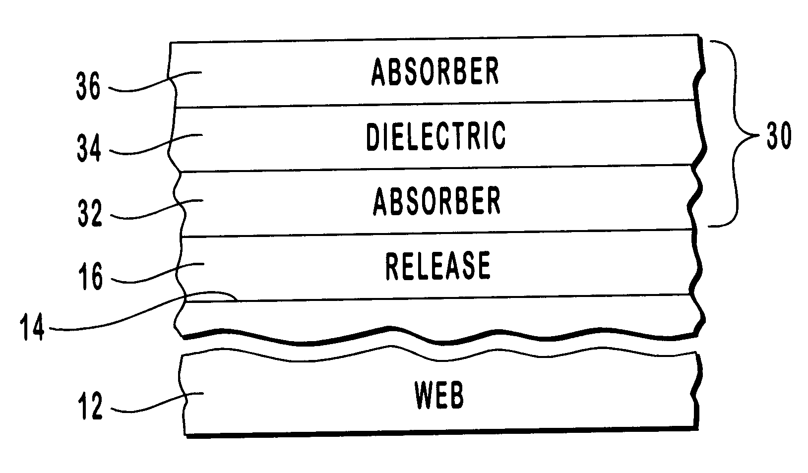
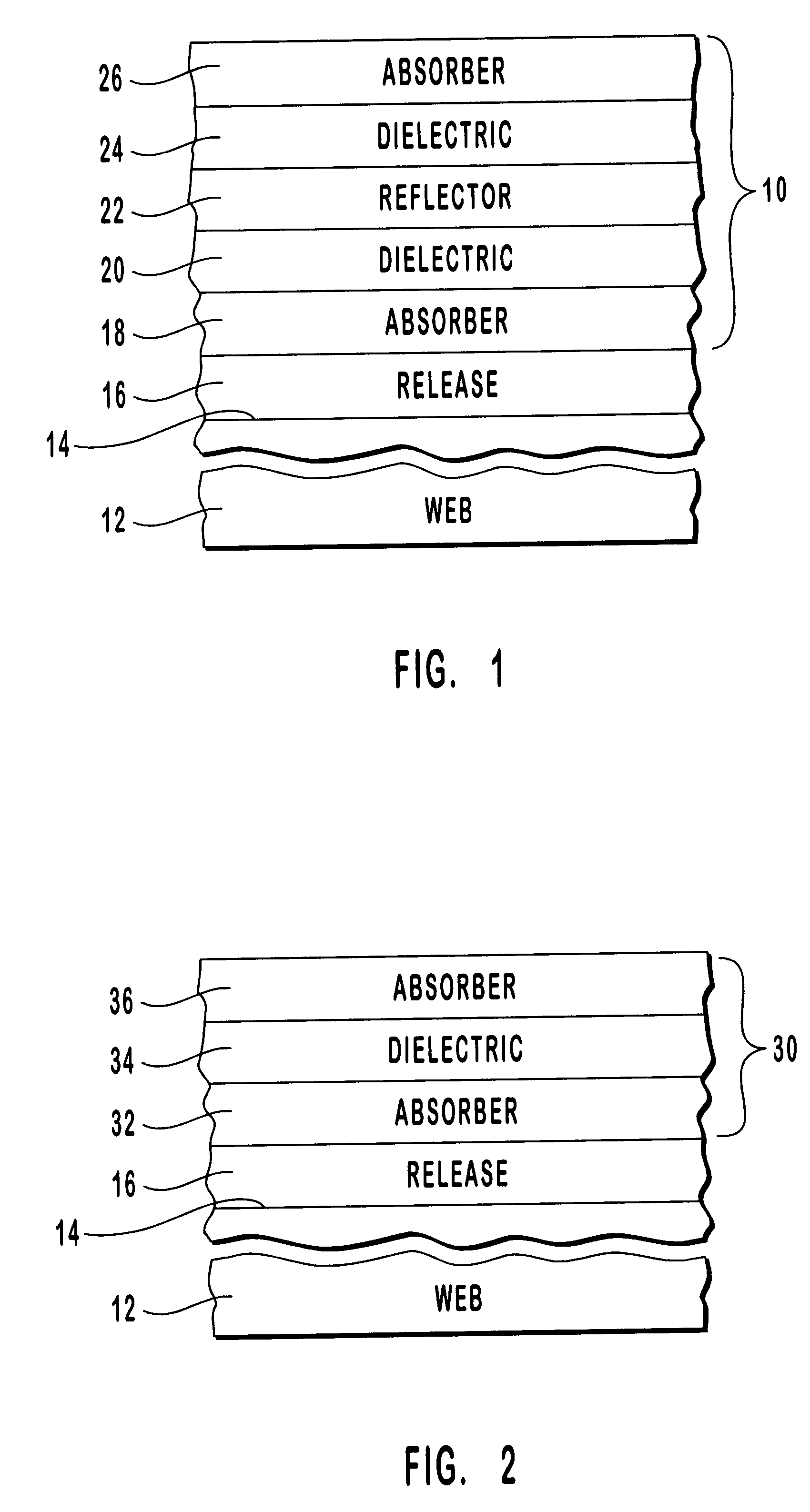
A color shifting interference film having a five layer design was fabricated according to the present invention by depositing an absorber layer composed of chromium 75 .ANG. thick on a web, followed by a first dielectric layer composed of zinc sulfide having a 5 QWOT at 535 nm. Upon the first dielectric layer was deposited a highly reflective layer of aluminum 800 .ANG. thick, followed by a second dielectric layer of zinc sulfide having a 5 QWOT at 535 nm. Lastly, another absorber layer of chromium 75 .ANG. thick was deposited on the second dielectric layer and the formed film was removed from the web. The zinc sulfide used in this particular design had a refractive index of about 2.2, and the number of the quarter wave optical thickness for the zinc sulfide was optimized for a design wavelength of 535 nm. The formed film had gold-to-green color shifting properties.
Table 2 below lists the values for the measured L*a*b* coordinates and .DELTA.E.sub.ab for the gold-to-green film desig...
example 2
A color shifting interference film having a five layer design similar to the interference film of Example 1 was fabricated according to the present invention. An absorber layer of chromium 75 .ANG. thick was deposited on a web, followed by a first dielectric layer of zinc sulfide having a 6 QWOT at 555 nm. Upon the first dielectric layer was deposited a highly reflective layer of aluminum 800 .ANG. thick, followed by a second dielectric layer of zinc sulfide having a 6 QWOT at 555 nm. Lastly, another absorber layer of chromium 75 .ANG. thick was deposited on the second dielectric layer. The formed interference film had green-to-magenta color shifting properties.
Table 3 below lists the values for the measured L*a*b* coordinates and .DELTA.E.sub.ab for the green-to-magenta film design of Example 2.
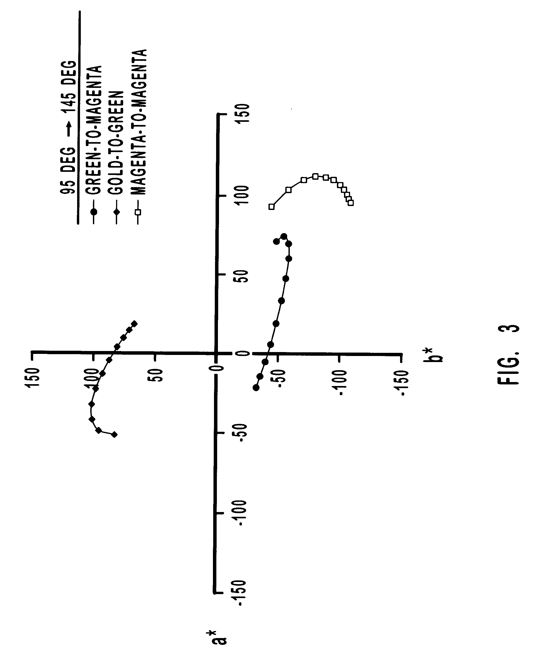
The measured color travel for the green-to-magenta film design is plotted in the graph of FIG. 3, in which the vector (arrow) represents the change in chroma and hue as the viewing angle cha...
example 3
A nonshifting color interference film having a five layer design was fabricated as a comparative example. An absorber layer of chromium 75 .ANG. thick was deposited on a web, followed by a first dielectric layer of zinc sulfide having a 4 QWOT at 506 nm. Upon the first dielectric layer was deposited a highly reflective layer of aluminum 800 .ANG. thick, followed by a second dielectric layer of zinc sulfide having a 4 QWOT at 506 nm. Lastly, another absorber layer of chromium 75 .ANG. thick was deposited on the second dielectric layer. The formed interference film had nonshifting magenta-to-magenta color properties.
Table 4 below lists the values for the measured L*a*b* coordinates and .DELTA.E.sub.ab for the magenta film design of Example 3.
The measured color travel for the magenta film design is plotted in the graph of FIG. 3, in which the vector (arrow) represents the change in chroma and hue as the viewing angle changes from 95 degrees to 145 degrees. As indicated in FIG. 3, while...
PUM
| Property | Measurement | Unit |
|---|---|---|
| physical thickness | aaaaa | aaaaa |
| optical thickness | aaaaa | aaaaa |
| optical thickness | aaaaa | aaaaa |
Abstract
Description
Claims
Application Information


