Semiconductor memory device

a memory device and semiconductor technology, applied in semiconductor devices, digital storage, instruments, etc., can solve the problems of slow data read operation, slow reading rate, slow data access operation,

Inactive Publication Date: 2002-01-15
NEC ELECTRONICS CORP
View PDF5 Cites 99 Cited by
  • Summary
  • Abstract
  • Description
  • Claims
  • Application Information

AI Technical Summary

Benefits of technology

The objective of this patent is to create a semiconductor memory device that ensures the same input impracticality between different cells within the main or reference arrays when measured by the sensing circuitry.

Problems solved by technology

The technical problem addressed in these prior art documents relates to improving the performance and reliability of analog-to-digital converters used in semiconductor memory devices. More specifically, they focus on solving issues related to differences in impodges and current levels caused by varying conditions such as temperature and process variations. Additionally, both methods aim to address difficulties associated with comparing signals and ensuring accurate detection of data bits.

Method used


Image

  • Semiconductor memory device
  • Semiconductor memory device
  • Semiconductor memory device

Examples


Embodiment Construction

Referring to the drawings, the embodiments of the present invention will be described in the following.

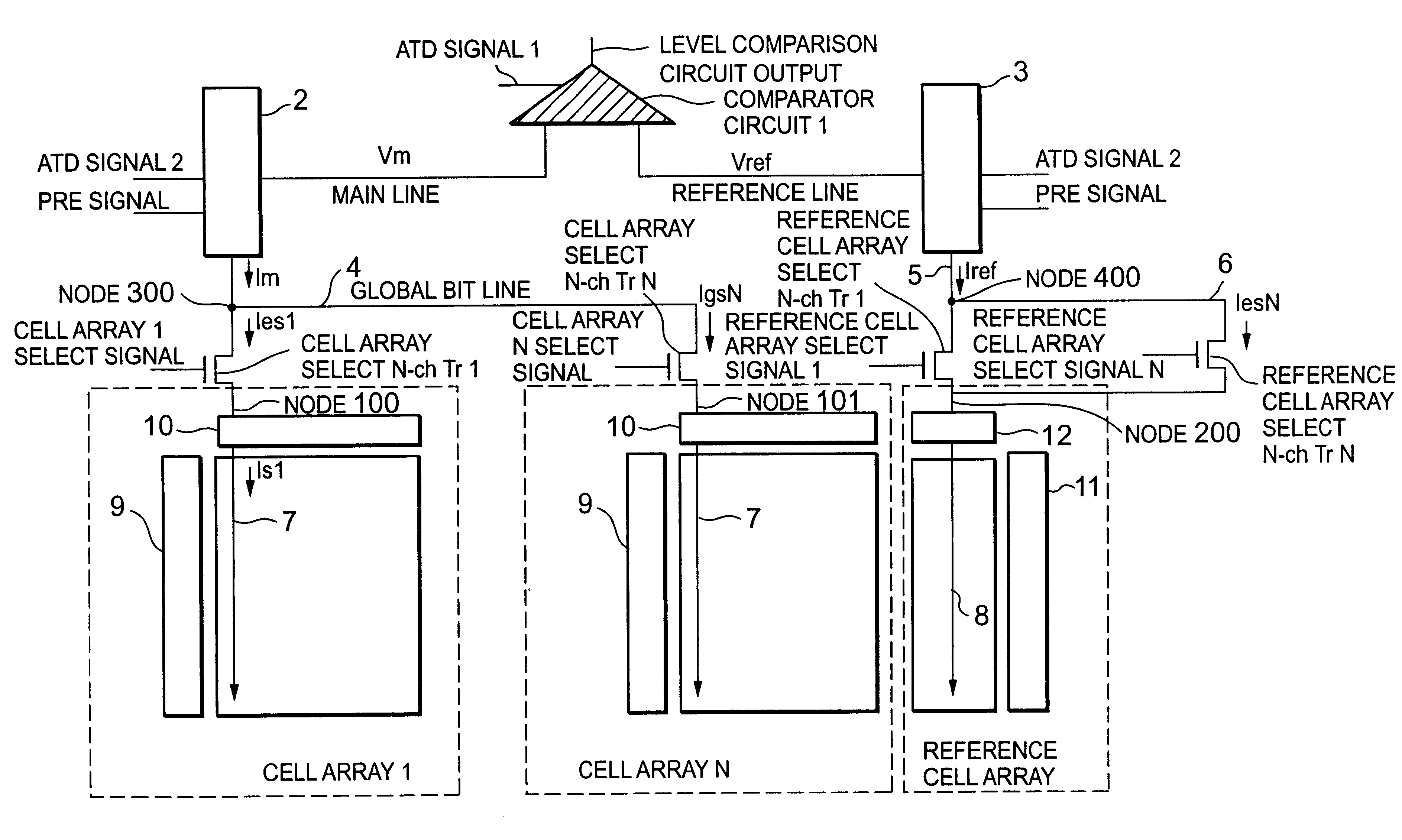
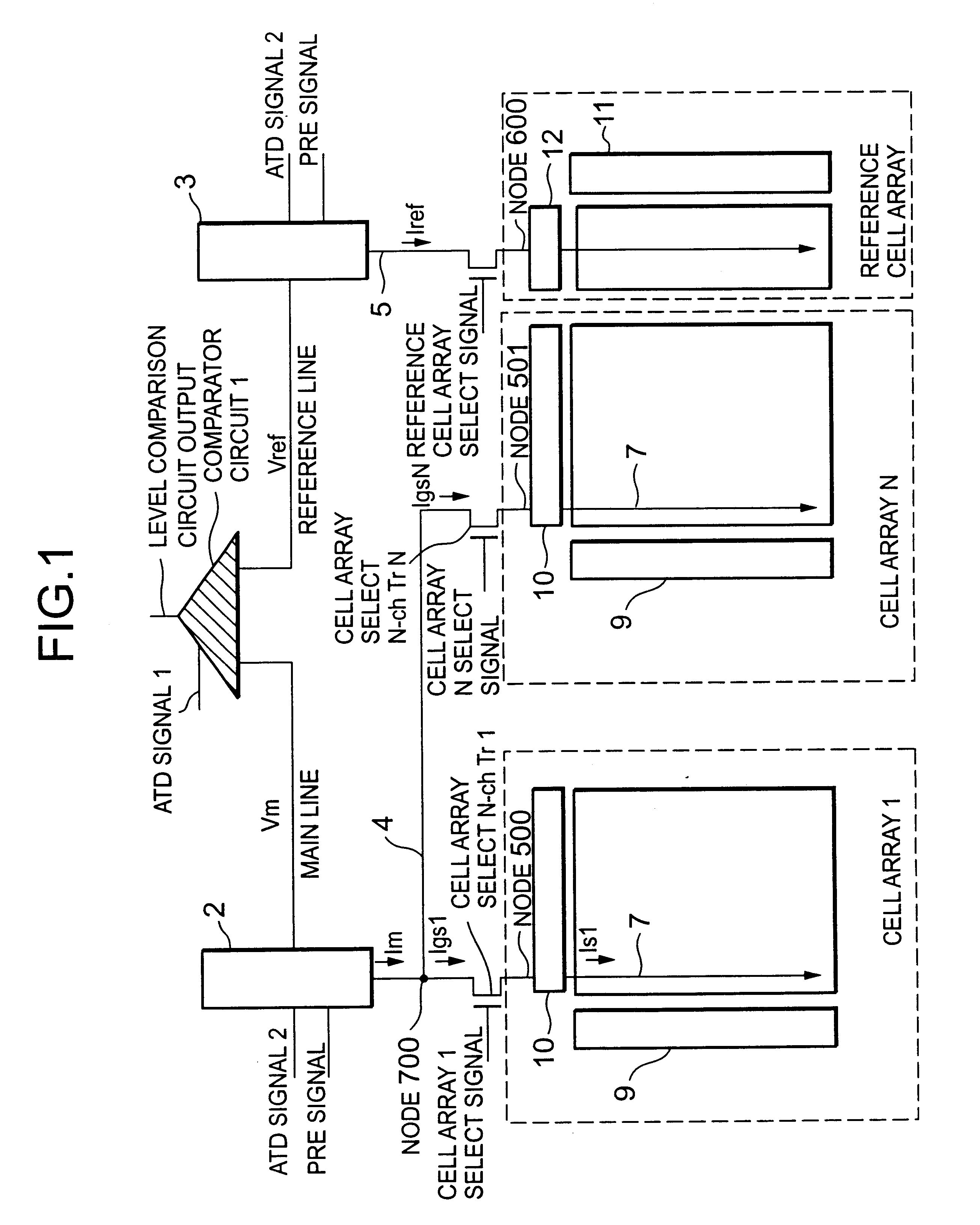
Referring to FIG. 2, FIG. 3, FIG. 5, FIG. 6 and FIG. 7, the configuration of a first embodiment of the semiconductor memory device according to the present invention will be described. FIG. 5 is a circuit diagram showing the configuration of a nonvolatile semiconductor memory device of the invention. The semiconductor memory device comprises a comparator circuit 1, an I-V conversion circuit 2, an I-V conversion circuit 3, a plurality of cell arrays (1 to N), and one reference cell array. Each cell array is equipped with a row decoder 9 (1 to N) and a column decoder 10 for selecting an arbitrary cell within a cell array. The reference cell array is equipped with a row decoder 11 and a dummy decoder 12.

The comparator circuit 1 inputs the output Vm of the I-V conversion circuit 2, the output Vref of the I-V conversion circuit 3 and outputs the result of level comparison to a control p...


PUM


Abstract

A semiconductor memory device having a plurality of cell arrays and one reference cell array according to the present invention includes a first current-to-voltage converting means that converts a cell current input from a cell array into a main cell voltage, a second current-to-voltage converting means that converts a reference cell current input from the reference cell array into a reference cell voltage, a global bit line that connects the first current-to-voltage converting means and the plurality of cell arrays, and a dummy global bit line that connects the second current-to-voltage converting means and the reference cell array, wherein the impedance of the global bit line is equal to the impedance of the dummy global bit line.

Description


Claims


Application Information

Patent Timeline
Owner NEC ELECTRONICS CORP
Why Eureka
Try Eureka