Shielded electronic circuit

a shielding and electronic circuit technology, applied in the field of shielded electronic circuits, can solve the problems of excessively different distances between shieldings, relative high mounting effort, and insufficient thermal conduction

Inactive Publication Date: 2003-07-08
MANNESMANN VDO AG
View PDF13 Cites 31 Cited by
  • Summary
  • Abstract
  • Description
  • Claims
  • Application Information

AI Technical Summary

Benefits of technology

The configuration of the outer shielding eliminates the actual cause of the problem of poor cooling of the inner shielding, namely the enclosure of the electronic component within the inner shielding by two walls. The inventive opening in the outer shielding allows the inner shielding in the vicinity of the opening to form a part of the wall face of the outer shielding. For this reason, heat from the inner shielding is emitted directly to the outside. Accordingly, the transmission of heat out of the inner shielding into the outer shielding is no longer required.
To properly shield a component, the gaps between the outer shielding and the inner shielding have to be dimensioned with regard to the wave lengths of the interfering frequencies. This causes difficulties because it is not possible to predict accurately with which regions the outer shielding will rest on the inner shielding. These uncertainties are avoided by arranging spherical impressions on the outer shielding such that the outer shielding rests on the inner shielding along the edge of the opening via the spherical impressions and the distances of the spherical impressions are matched to the wave lengths of the interfering frequencies.
A particularly good cooling effect and at the same time an overall volume which is as small as possible is obtained if the inner shielding is higher than the outer shielding relative to a main printed circuit board of the electronic circuit and the Z-shaped tongues of the outer shielding are led upward out of the plane of the outer shielding to the plane of the inner shielding.

Problems solved by technology

If the inner shielding is provided within the outer shielding, the conduct of the heat of the electronic components which are doubly shielded in this way causes difficulties.
However, such a connection of the shieldings via, for example, a thermally conductive rubber entails a relatively high degree of effort in terms of mounting and requires tight tolerances of the components so that excessively differing distances between the two shieldings have to be bridged.
Furthermore, the resulting thermal conduction is often inadequate because the heat must first pass from the one shielding into the thermal conductive rubber and then from the thermally conductive rubber into the other shielding before the outer shielding can emit the heat into the ambient air.
This causes difficulties because it is not possible to predict accurately with which regions the outer shielding will rest on the inner shielding.

Method used


Image

  • Shielded electronic circuit
  • Shielded electronic circuit

Examples


Embodiment Construction

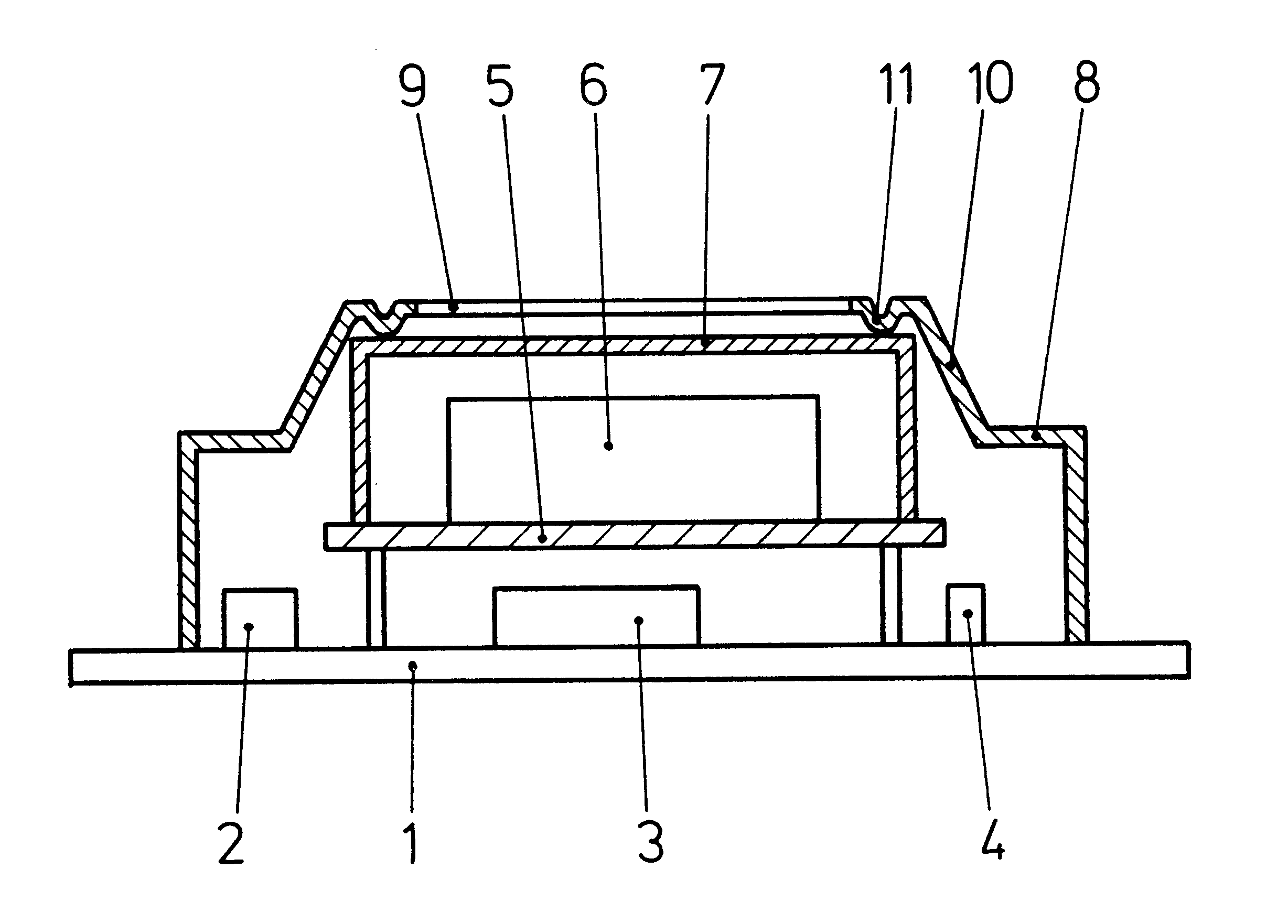
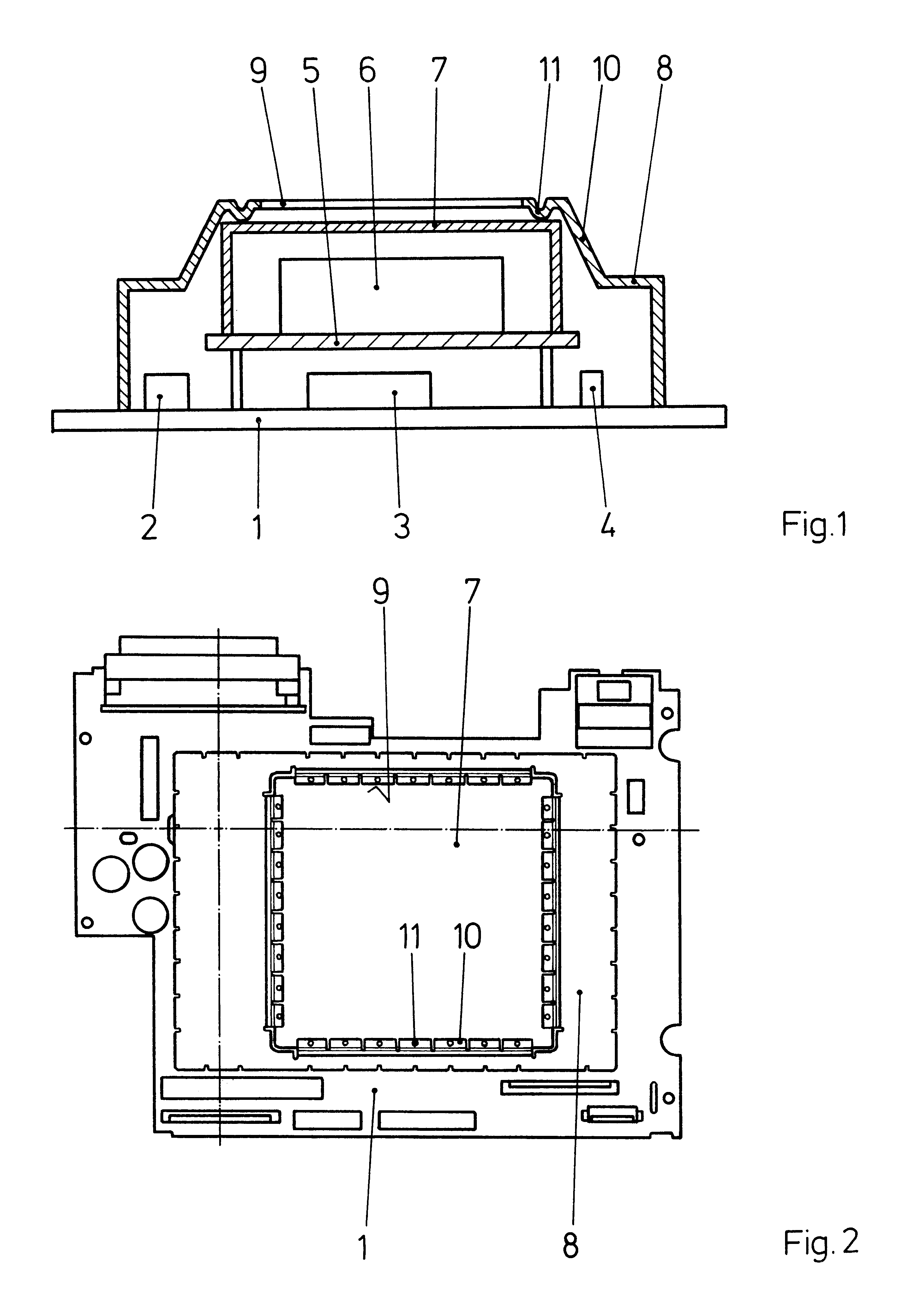
A main printed circuit board 1 is shown in FIG. 1 on which various circuit components 2, 3, 4 are arranged. An auxilliary printed circuit board 5 with an electronic component 6 is also mounted on the main printed circuit board 1 at a distance from the main printed circuit board 1 and parallel to the main printed circuit board 1. The electronic component 6 is encapsulated by an inner shielding 7 mounted on the secondary circuit board 5. An outer shielding 8 mounted on the main circuit board 1 covers the entire electronic circuit. The outer shielding has an opening 9 bounded by spring tongues 10 which extend upward from the outer shielding in a Z-shape. Each of the spring tongues 10 includes a spherical impression 11 which rests under tension on an upper side of the inner shielding 7.

FIG. 2 shows the main printed circuit board 1 with the outer shielding 8 arranged on it. Furthermore, the opening 9 bounded by the spring tongues 10 is clearly shown. Each spring tongue 10 rests under ten...


PUM


Abstract

An electronic circuit includes an outer shielding mounted on a main printed circuit board. To prevent electronic components from affecting one another, at least one inner shielding is arranged within the outer shielding. The outer shielding has an opening bounded by spring tongues which rest on the inner shielding.

Description

1. Field of the InventionThe present invention relates to an electronic circuit with an outer shielding and at least an inner shielding within the outer shielding for preventing the electronic components of the electronic circuit from affecting one another.2. Description of the Related ArtElectronic circuits having a shielding are generally known and customary in technology such as, for example, in motor vehicles for vehicle application apparatus. The shielding protects the electronic components of the electronic circuit against external electromagnetic influence and prevents electromagnetic waves from irradiating outwards from the electronic circuit so the electronic circuit does not disrupt any external electronic devices. Electronic circuits often contain electronic components which may affect one another. For this reason, these circuits require an inner shielding of individual components within the outer shielding of the entire electronic circuit. If the inner shielding is provi...

Claims


Application Information

Patent Timeline
Patent Type & Authority Patents(United States)
IPC IPC(8): H05K9/00
CPCH05K9/0024Y10S174/35H05K9/0032
Inventor SPRATTE, JOACHIMREINHARDT, JORG
Owner MANNESMANN VDO AG
Why Eureka
Try Eureka