Display device comprising substrates, contrast medium and barrier layers between contrast medium and each of substrates

a technology of contrast medium and substrate, which is applied in the manufacture of final products, identification means, instruments, etc., can solve the problems of difficult to maintain flatness of the plate surface, deterioration of liquid crystals, and offensive flickering, so as to reduce costs, increase production efficiency, and supply a large amount of display media.

Inactive Publication Date: 2005-04-26
SEMICON ENERGY LAB CO LTD
View PDF23 Cites 135 Cited by
  • Summary
  • Abstract
  • Description
  • Claims
  • Application Information

AI Technical Summary

Benefits of technology

[0020]Among the above steps, the second to ninth steps are for forming based on the screen-printing method, making it possible to supply a display medium having a large area in large amounts and at decreased costs like printing characters and photographs on a paper without relying upon the vacuum technology such as vapor growth or the photo...

Problems solved by technology

Further, when continuously driven on direct current drive, the liquid crystals are deteriorated.
When the frequency of inversion is low, however, there appears flickering which is offensive to see.
Further, in order for the users to enjoy the convenience of handling, it is not desired to use, as a substrate, brittle...

Method used


Image

  • Display device comprising substrates, contrast medium and barrier layers between contrast medium and each of substrates
  • Display device comprising substrates, contrast medium and barrier layers between contrast medium and each of substrates
  • Display device comprising substrates, contrast medium and barrier layers between contrast medium and each of substrates

Examples


Embodiment Construction

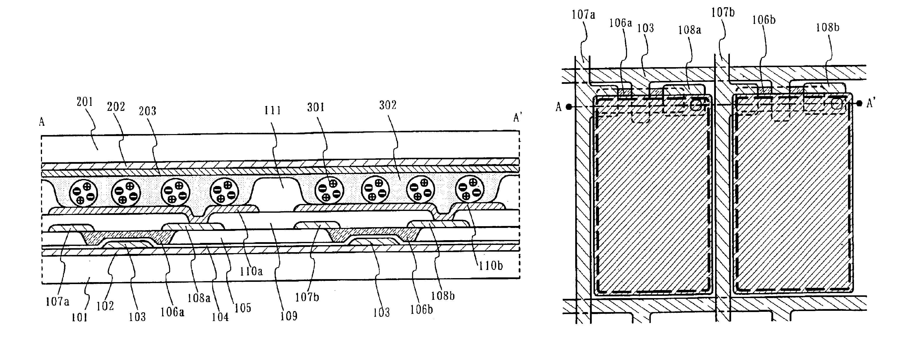
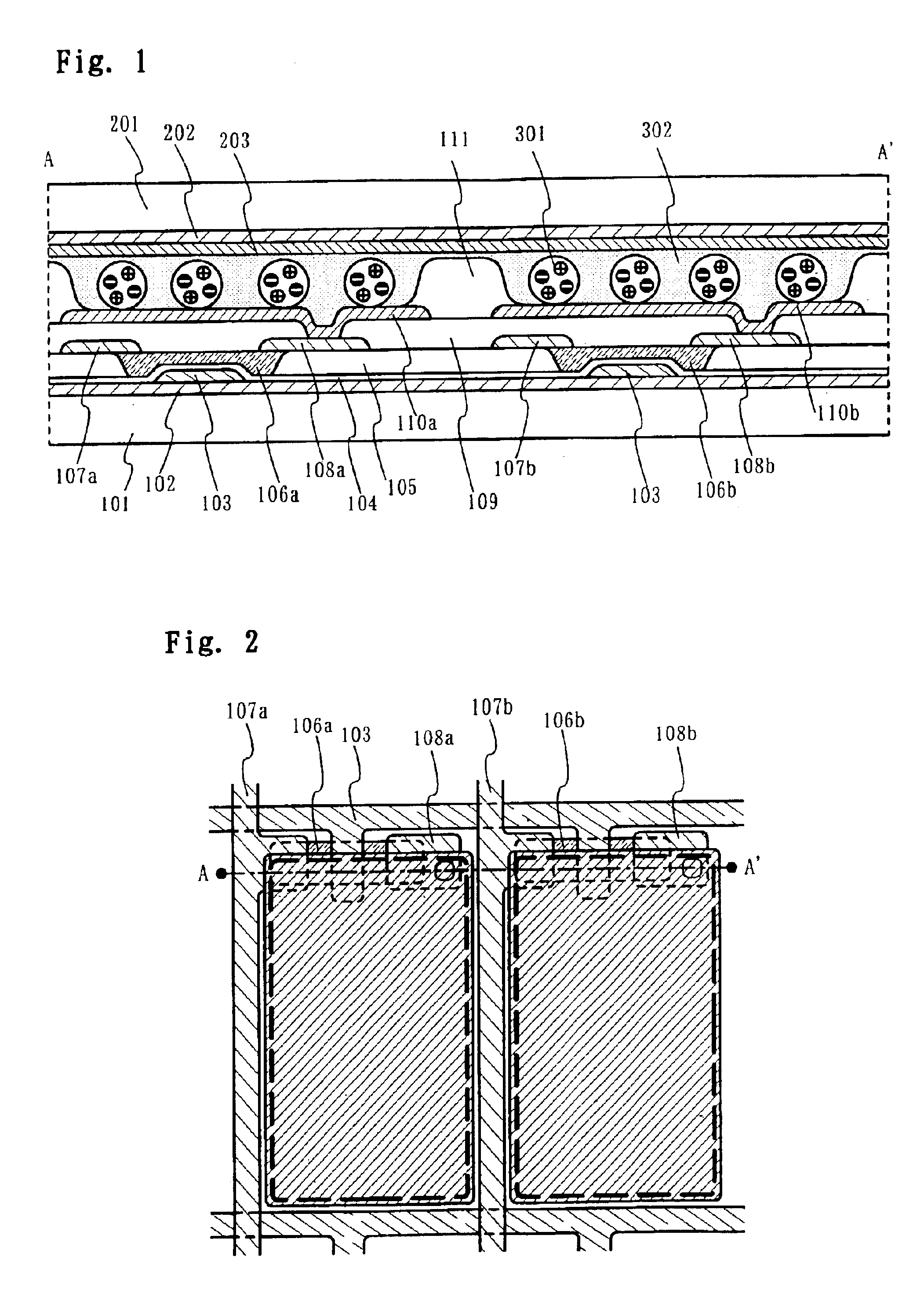
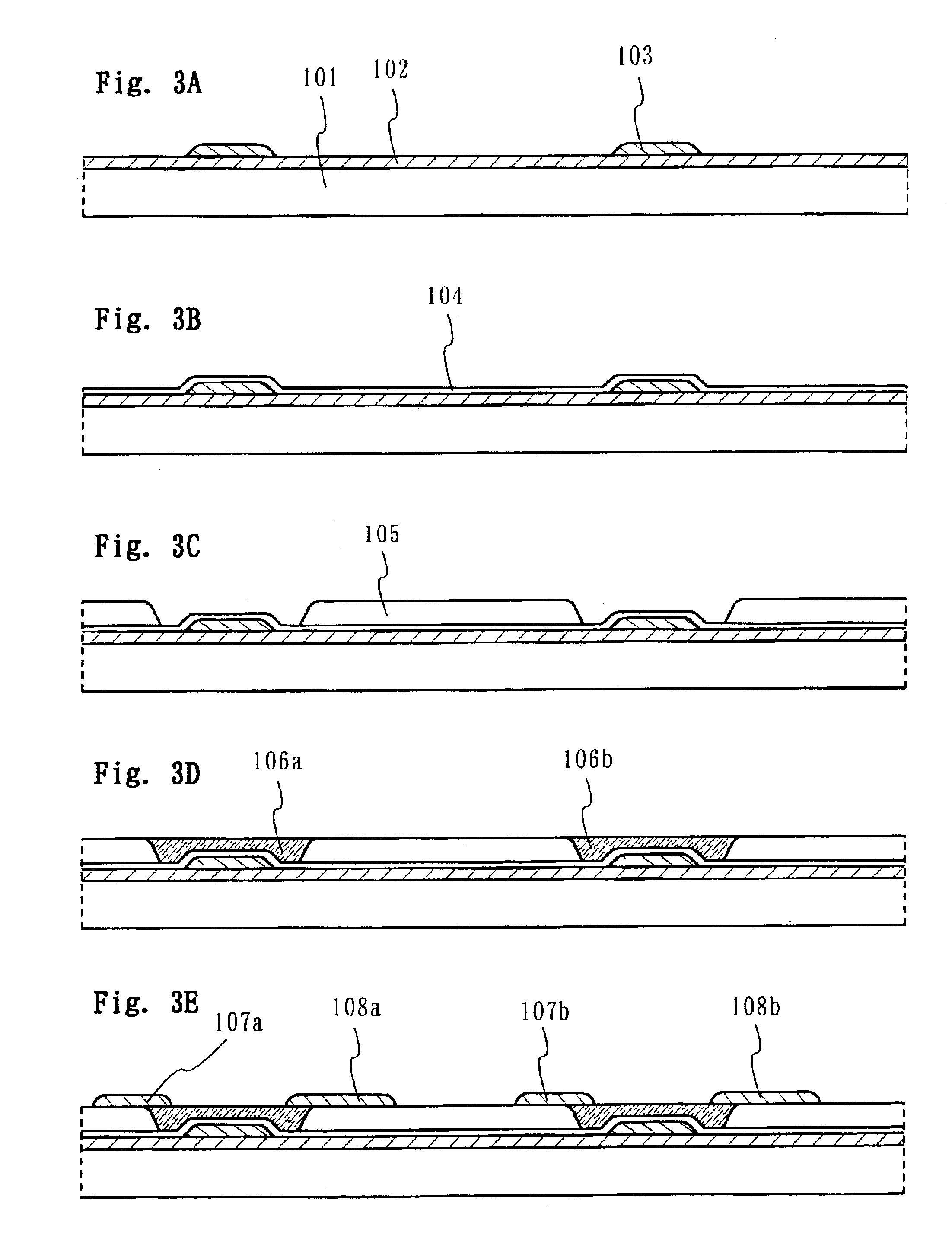
[0032]Embodiments of the invention will now described in detail with reference to the drawings. The display device according to the invention includes a pixel unit equipped with contrast media which change the reflectivity upon the application of an electric field or an electronic ink including microcapsules containing electrically charged particles that change the reflectivity upon the application of an electric field, for each of the pixels, the pixel unit further having TFTs for controlling the electric field to be applied to each of the pixels. In the TFTS, an organic semiconductor material is used as a semiconductor for forming channel portions, wherein a feature resides in the structure for separating the semiconductor in the form of islands and in the method of fabrication. The thus constituted pixel unit is sandwiched by the plastic substrates.

[0033]FIG. 1 is a vertical sectional view illustrating the structure of the pixel unit, and FIG. 2 is a top view thereof. Between pla...


PUM


Abstract

A constitution of the display device of the invention is shown in the following. The display device includes a pixel unit including TFTs of which the active layer contains an organic semiconductor material for forming channel portions in the opening portions in an insulating layer arranged to meet the gate electrodes. The pixel unit further includes a contrast media formed on the electrodes connected to the TFTs for changing the reflectivity upon the application of an electric field, or microcapsules containing electrically charged particles that change the reflectivity upon the application of an electric field. The pixel unit is sandwiched by plastic substrates, and barrier layers including an inorganic insulating material are provided between the plastic substrates and the pixel unit. The purpose of the present invention is to supply display devices which are excellent in productivity, light in weight and flexible.

Description

BACKGROUND OF THE INVENTION[0001]1. Field of the Invention[0002]This invention relates to a display device using contrast media which change the reflectivity upon the application of an electric field. In particular, the invention relates to a display device formed by combining a substrate of an organic resin film with thin film transistors (hereinafter referred to as TFTs) and the contrast media, as well as to a method of fabricating the same.[0003]2. Description of the Related Art[0004]Unlike means that uses a cathode-ray tube, a display device that forms a screen on a flat plate is designed to give electric signals to pixels which are arranged in nearly a two-dimensional manner, and to impart brightness and density by utilizing electro-optical properties of liquid crystals or light-emitting properties of electroluminescence medium, thereby to display an image. Attention has now been given to the display device of this kind which is a new type of display medium by using an electrop...

Claims


Application Information

Patent Timeline
IPC IPC(8): G02F1/01G02F1/167G02F1/16757G02F1/16766G02F1/1677
CPCG02F1/167G02F1/16757G02F1/1677G02F1/16766Y02E10/549Y02P70/50G02B26/026G09F9/372G09G3/344G02F1/1681H10K10/466H10K77/111G02F1/133305G02F1/1368G02F2001/1678G02F2201/123
Inventor YAMAZAKI, SHUNPEIARAI, YASUYUKI
Owner SEMICON ENERGY LAB CO LTD
Why Eureka
Try Eureka