Land grid array socket loading device

a technology of sockets and loading devices, applied in the direction of coupling device connections, non-rotary current collectors, electrical apparatus construction details, etc., can solve the problem of limiting the overall practical number of pins of a given package that may be supported

Inactive Publication Date: 2005-07-12
INTEL CORP
View PDF9 Cites 42 Cited by
  • Summary
  • Abstract
  • Description
  • Claims
  • Application Information

AI Technical Summary

Benefits of technology

[0007]The objects, features, and advantages of the invention as hereinafter claimed will be apparent to one skilled in the art in view of the following detailed description in which:

Problems solved by technology

However, increasing the number of electrical connections for a given IC presents the challenge of finding a way to accommodate having an increasing number of contacts mounted on an IC package in a way that will still afford a practical way to attach the IC package (and thereby, attach the IC within) to a circuitboard so that electrical connections with other devices are created.
However, there are other situations where the IC must be removably attached to a circuitboard such that an unskilled user of a product in which the circuitboard is installed must be able to attach or detach the IC from the circuitboard without the benefit of a host of specialized tools.
In such situations, it is seldom deemed acceptable or desirable to require such a user to solder or desolder an IC encapsulated within a package having a very large number of contacts, and so the use of a socket by which the IC may be removably attached to a circuitboard must be provided for.
This requires mechanisms within the socket that limits the possible density of pins and thereby limits the overall practical number of pins on a given package that may be supported.
Unfortunately, the pressure required to press each pin of a socket against each corresponding pin of a package requires a certain quantity of force to ensure a good electrical connection, and this pressure is cumulative, such that the amount of force required goes up with the number of pairs of corresponding contacts that must be pressed together.
This cumulative amount of force can pose various mechanical design challenges, including the need to evenly spread the force across all of the corresponding pairs of pins to ensure that each receives the required amount of force without receiving an excessive quantity of force.

Method used


Image

  • Land grid array socket loading device
  • Land grid array socket loading device
  • Land grid array socket loading device

Examples


Embodiment Construction

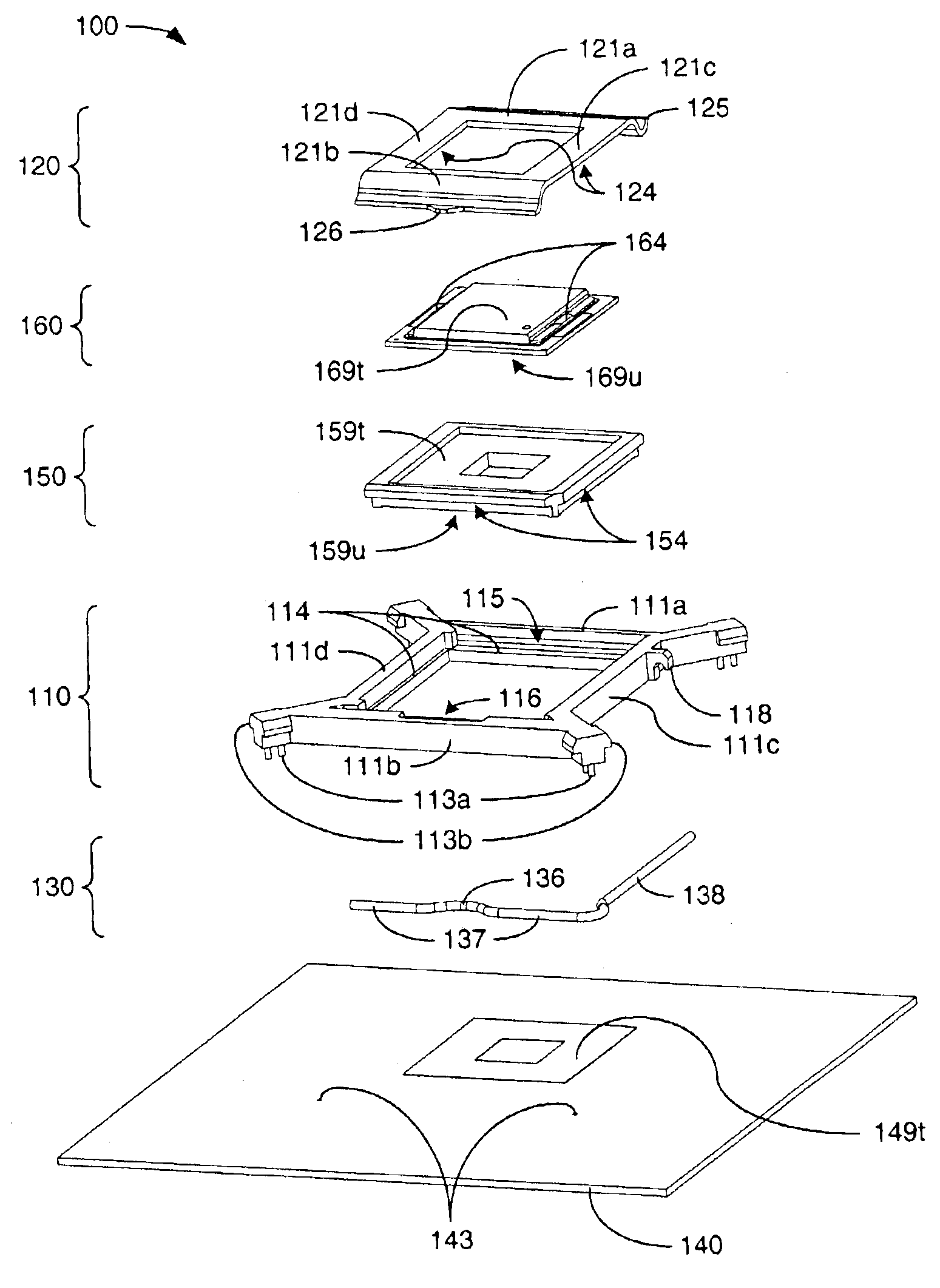
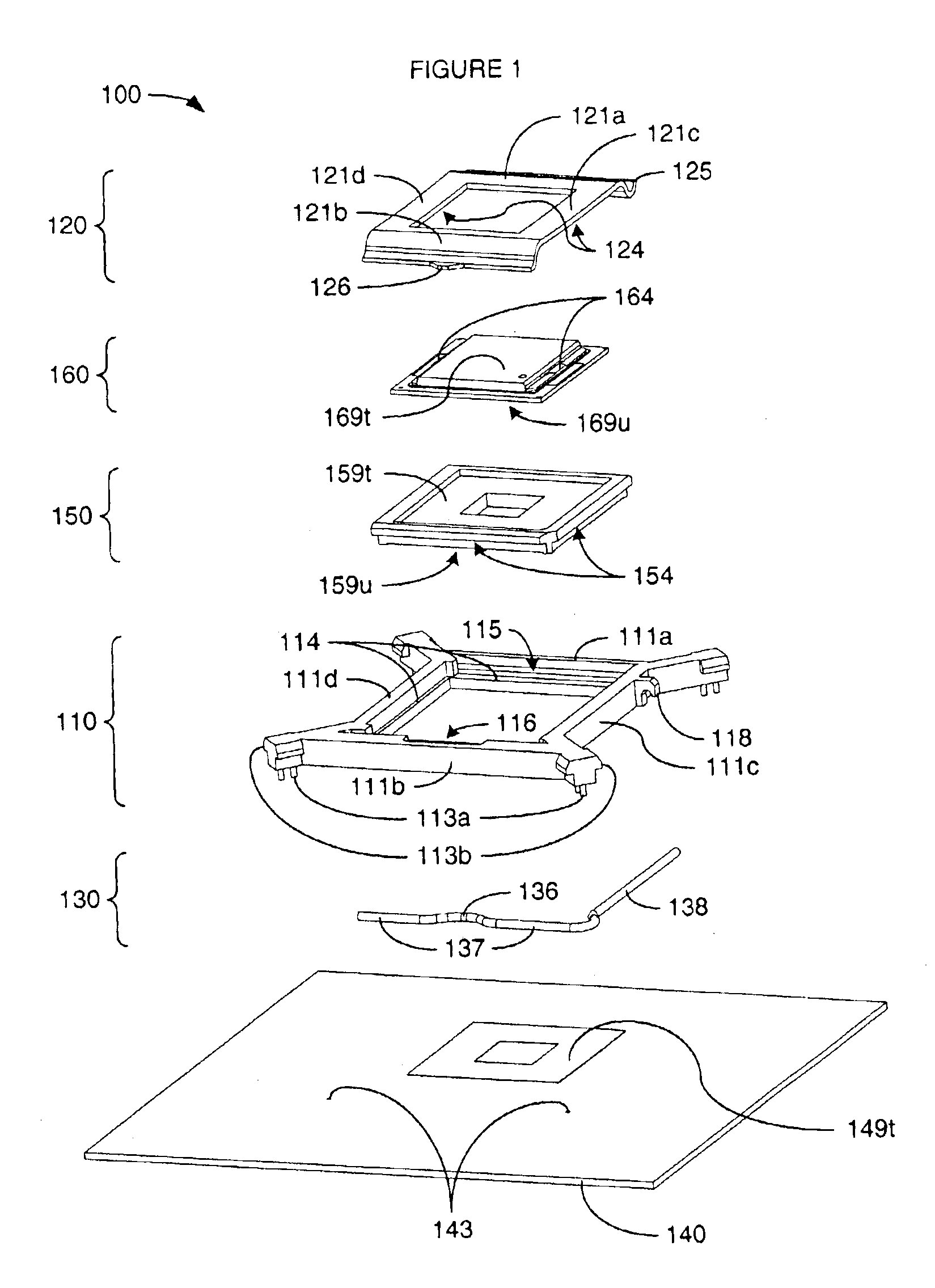
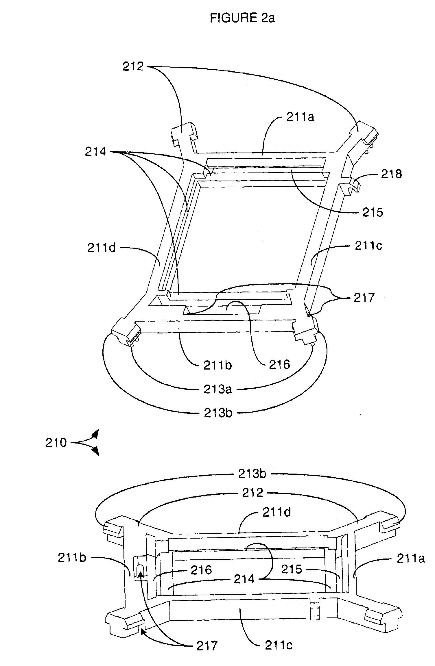
[0020]Although numerous details are set forth for purposes of explanation and to provide a thorough understanding in the following description, it will be apparent to those skilled in the art that these specific details are not required in order to practice embodiments of the invention as hereinafter claimed. For example, although embodiments are discussed with reference to an IC device having a package with land grid array (LGA) contacts, it will be readily apparent to those skilled in the art that other embodiments having other types of contacts may be employed without departing from the spirit and scope of the invention as hereinafter claimed.

[0021]Apparatus for removably retaining an IC package in engagement with a socket such that the contacts of both the IC package and the socket are properly engaged is disclosed. Specifically, a frame that engages a socket and a load plate that engages an IC package are caused to press the socket and IC package together through force selectiv...


PUM


Abstract

A method and an apparatus for removably retaining an IC in engagement with a socket such that contacts carried by the package of the IC are pressed into engagement with contacts carried by the socket by way of a retention frame with ledges positioned opposite corresponding ledges of the socket and both a load plate and load lever pivotally connected to the retention frame.

Description

FIELD OF THE INVENTION[0001]An apparatus for retaining an IC device encapsulated within a land grid array package in electrical contact with a socket.ART BACKGROUND[0002]As part of continuing efforts to increase the functionality of integrated circuits (ICs) such as central processing units (CPUs), there has been a continuing need to provide ever more electrical contacts (commonly referred to as “pins”) on the packages in which ICs are typically encapsulated to enable ever greater interactions between such ICs and other devices. However, increasing the number of electrical connections for a given IC presents the challenge of finding a way to accommodate having an increasing number of contacts mounted on an IC package in a way that will still afford a practical way to attach the IC package (and thereby, attach the IC within) to a circuitboard so that electrical connections with other devices are created.[0003]In answer to this increasing need to provide more electrical contacts for u...

Claims


Application Information

Patent Timeline
Patent Type & Authority Patents(United States)
IPC IPC(8): H01R12/00H01R12/16H05K7/10
CPCH05K7/1061H01R12/7076H01R12/88
Inventor BYQUIST, TOD A.
Owner INTEL CORP
Why Eureka
Try Eureka