
Brush scrubbing-high frequency resonating wafer processing system and methods for making and implementing the same

a technology of high frequency resonating wafers and processing systems, applied in the direction of cleaning using liquids, vehicle cleaning, photosensitive materials, etc., can solve the problems of affecting the performance of integrated circuit devices, brush scrubbing operations can generally only dislodge contaminants defined on planer surfaces, and brush scrubbing operations may exhibit a rather poor cleaning capacity

Inactive Publication Date: 2005-10-04
LAM RES CORP
View PDF5 Cites 50 Cited by
  • Summary
  • Abstract
  • Description
  • Claims
  • Application Information

AI Technical Summary

Benefits of technology

The technical effect of this patent is that it describes how an improved system can be created for controlling electronic devices based on their movement or position within a space. This allows for more precise control over these devices without requiring them to constantly communicate with external sensors or processors.

Problems solved by technology

The technical problem addressed in this patent text is the limited effectiveness of current methods of cleanning semiconductor device wafers during manufacturing. Current techniques like brush scratching and megasonic cleaning leave behind contaminants that cannot always be completely removed, leading to incomplete cleaning results. Additionally, separate equipment and procedures are required for individual steps involved in the cleaning process, resulting in longer production times and decreased productivity. There is also a need for a method and apparatus that combines both brush scattering and megasonic cleaning to produce a simultaneous removal of contaminants from the wafer surface and interior topology without increasing the number of standalone modules needed for cleaning.

Method used


Image

  • Brush scrubbing-high frequency resonating wafer processing system and methods for making and implementing the same
  • Brush scrubbing-high frequency resonating wafer processing system and methods for making and implementing the same
  • Brush scrubbing-high frequency resonating wafer processing system and methods for making and implementing the same

Examples


Embodiment Construction

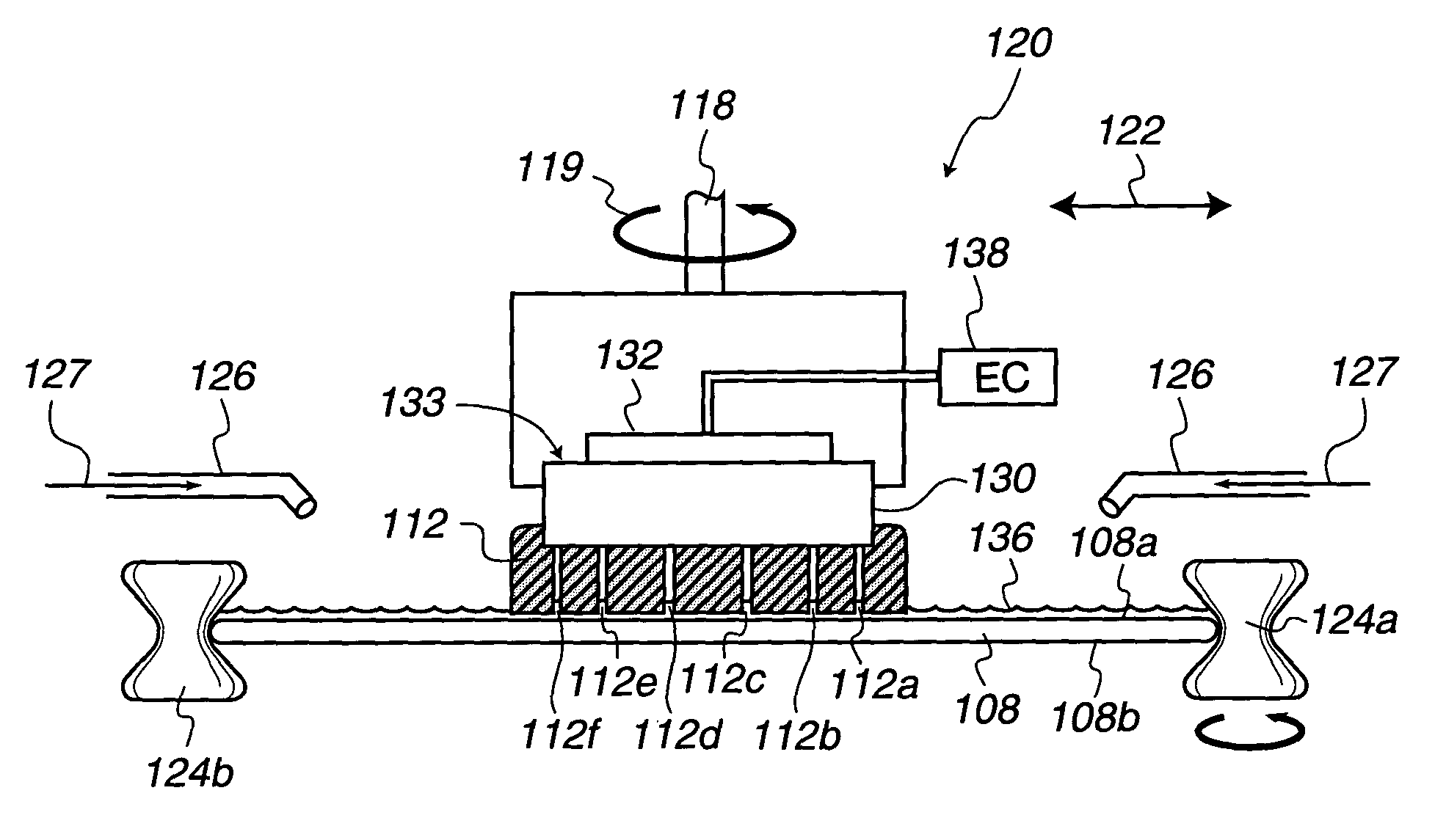
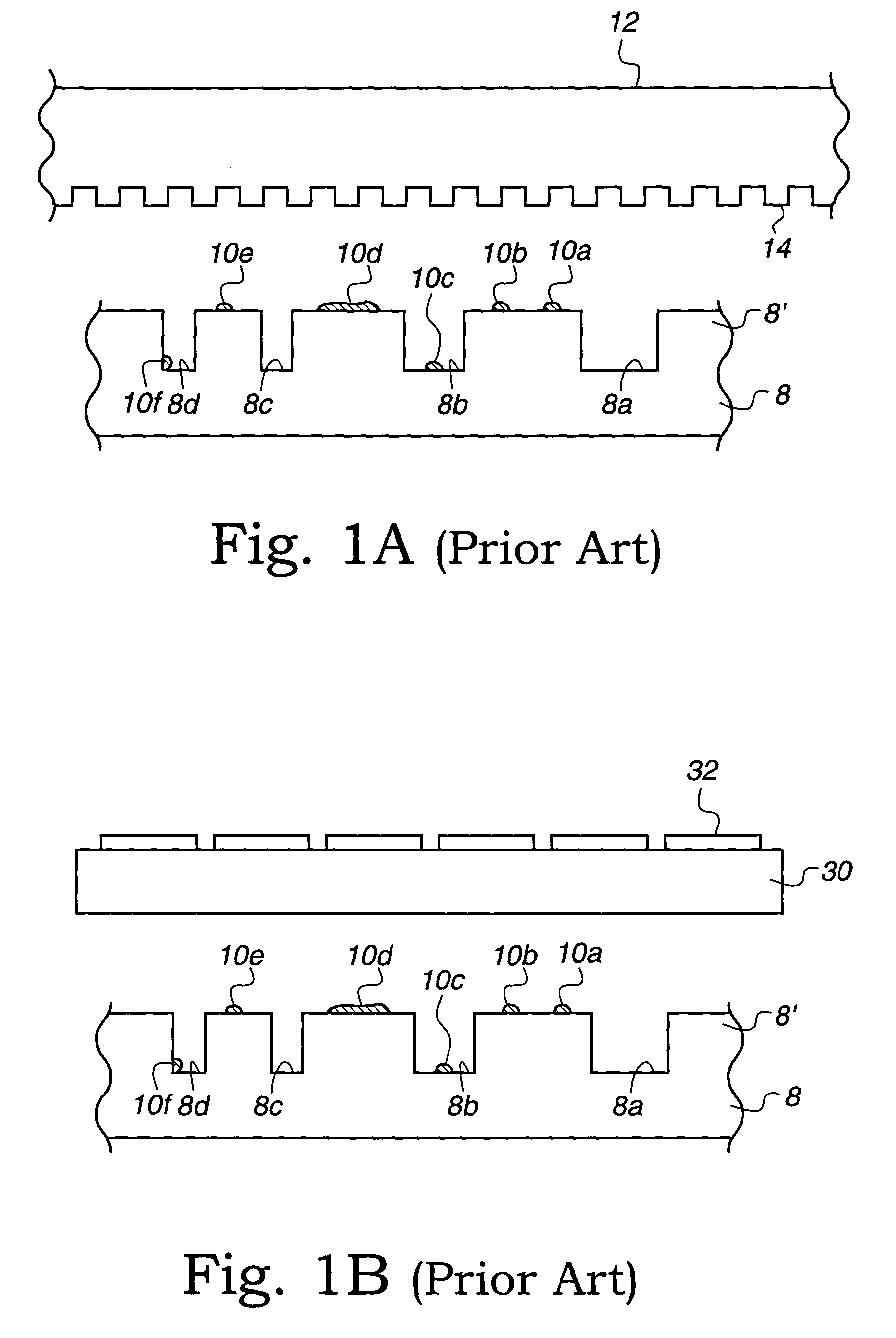
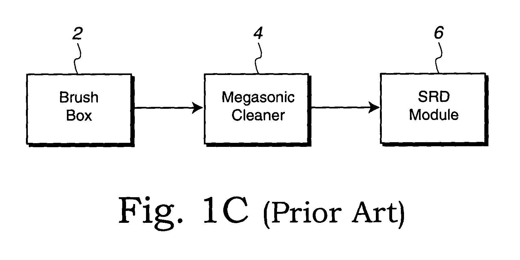
[0046]Several exemplary embodiments of the invention will now be described in detail with reference to the accompanying drawings. FIGS. 1A, 1B, and 1C are discussed above in the “Background of the Invention” section.

[0047]The embodiments of the present invention provide an apparatus and a method for cleaning a semiconductor substrate by concurrently using a combination of high frequency acoustic energy cleaning and brush scrubbing in a stand alone cleaning module. In one embodiment, a brush scrubbing-high frequency acoustic energy cleaning assembly capable of substantially removing contaminants lodged on wafer planer surfaces or deep wafer topography features. In one embodiment, a flat brush scrubbing-acoustic energy (AE) cleaning assembly is provided. The flat brush scrubbing-AE cleaning assembly includes a housing, a transducer having a crystal bonded to a resonator, and an arm configured to move the housing and thus the flat brush scrubbing-AE cleaning assembly. A flat brush havi...


PUM


Abstract

A substrate cleaning apparatus is provided. The apparatus includes a transducer capable of resonating at a high frequency and a brush material attached to a surface of the transducer. The brush material includes at least one passage extending to the surface of the transducer and is configured to be applied to a surface of a substrate. When the transducer resonates at the high frequency, the transducer is capable of imparting acoustic energy to the surface of the substrate at a location of the at least one passage.

Description


Claims


Application Information

Patent Timeline
Owner LAM RES CORP
Features
  • Generate Ideas
  • Intellectual Property
  • Life Sciences
  • Materials
  • Tech Scout
  • Unparalleled Data Quality
  • Higher Quality Content
  • 60% Fewer Hallucinations
Learn More