Method and apparatus for wafer cleaning

Inactive Publication Date: 2002-03-14
APPLIED MATERIALS INC
View PDF17 Cites 162 Cited by
  • Summary
  • Abstract
  • Description
  • Claims
  • Application Information

AI Technical Summary

Problems solved by technology

However, this method is not possible when the wafers have any topography (patterns) that can be damaged by the brushes.
When spray methods are used in this way, the sonic pressure waves are confined to the droplets of the spray where they then lose a lot of their power.
When the droplets hit the wafer surface, most of the remaining sonic energy is lost.
None of these attempts to apply megasonics to a single wafer surface is sufficiently efficient as they do not reduce the single wafer cleaning time enough, which is of the utmost importance.
Moreover, none of the current single wafer techniques are able to clean sufficiently both the front and the backside of the wafer at the same time.
Contamination left on the device side can cause a malfunctioning device.
Contamination left on the non-device side (backside) can cause a number of problems.
Backside contamination can cause the photolithography step on the front side to be out of focus.
Contamination on the backside can cause contamination of the processing tools, which

Method used


Image

  • Method and apparatus for wafer cleaning
  • Method and apparatus for wafer cleaning
  • Method and apparatus for wafer cleaning

Examples


Embodiment Construction

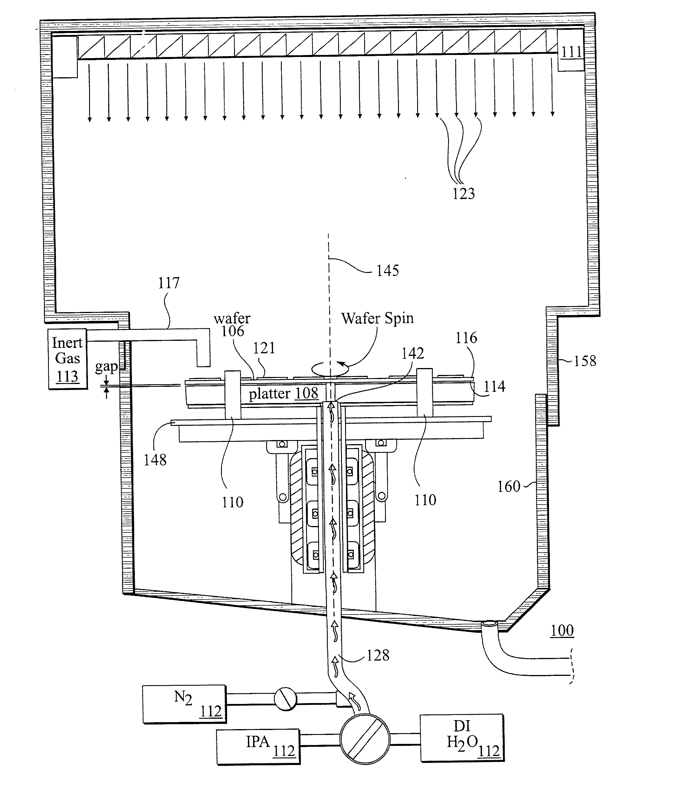
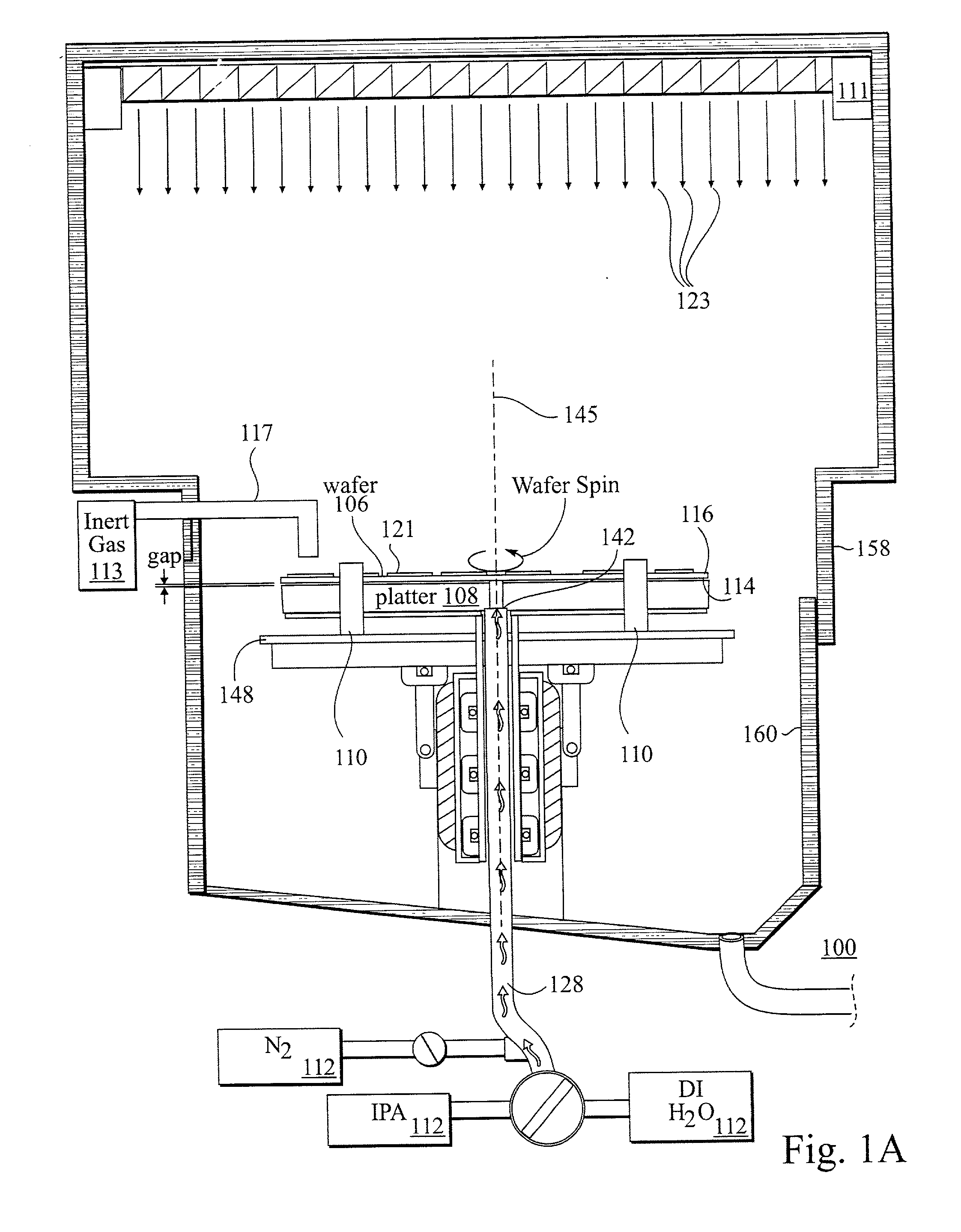
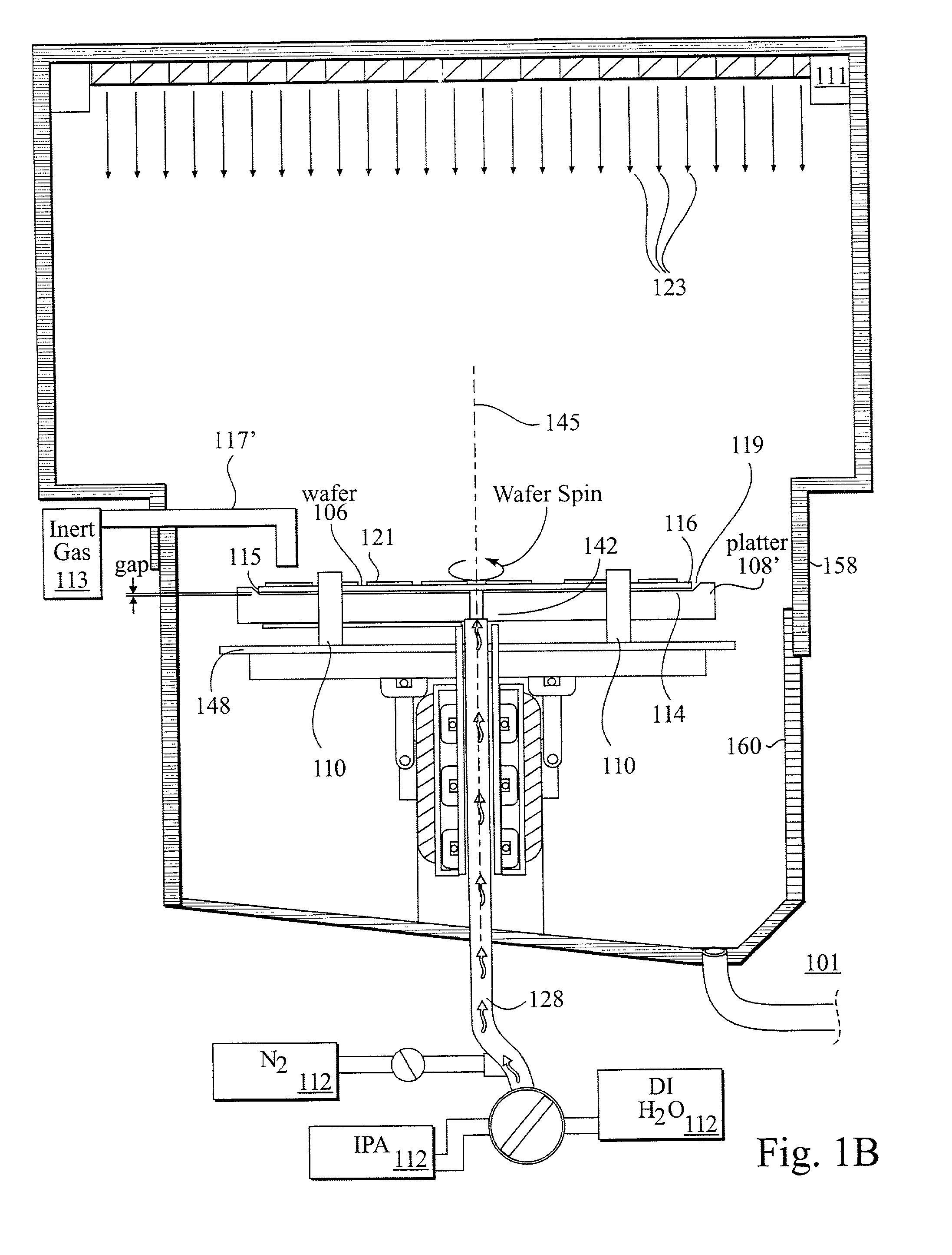
[0036] An apparatus and method of use to provide single wafer cleaning is disclosed. A process chamber (chamber) can process either or both a top and a bottom side of a single wafer in chip processing. The chamber can offer high wafer throughput along with good process control while providing low use of cleaning solutions.

[0037] In one embodiment, a single wafer is positioned in a wafer holding bracket (bracket) above a platter. Chemicals such as cleaning and rinse solutions are transferred through the platter from below to contact the bottom side of the wafer. Sufficient chemical flow is provided to fill a gap between the wafer and the platter. Once the gap is filled, little additional chemicals may be required, with the solution within the gap maintained in position by natural forces such as surface tension and capillary forces.

[0038] In another embodiment, a first group of chemicals (first chemical) are transferred to the bottom side of the wafer while chemicals from a different ...


PUM

PropertyMeasurementUnit
Lengthaaaaaaaaaa
Lengthaaaaaaaaaa
Lengthaaaaaaaaaa

Abstract

An apparatus for wet processing individual wafers comprising; a means for holding the wafer; a means for providing acoustic energy to a non-device side of the wafer; and a means for flowing a fluid onto a device side of the wafer.

Description

[0001] This application is a continuation-in-part of U.S. application Ser. No. 09 / 603,792, filed Jun. 26, 2000.[0002] 1. Field of the Invention[0003] The present invention relates to the field of cleaning of a substrate surface and more particularly to the area of chemical and megasonic cleaning of a semiconductor wafer.[0004] 2. Discussion of Related Art[0005] In semiconductor wafer substrate (wafer) cleaning, particle removal is essential. Particles can be removed by chemical means or by mechanical means. In current state of the art, particles are usually removed by both a combination of mechanical means and chemical means. The current state of the art is a batch process that places a number of wafers into a bath filled with a liquid and to apply high frequency (megasonic) irradiation to the liquid. Megasonic cleaning uses a ceramic piezoelectric crystal excited by a high-frequency AC voltage that causes the crystal to vibrate. The vibration causes sonic waves to travel through th...

Claims


Application Information

Patent Timeline
IPC IPC(8): B08B3/02B08B3/12H01L21/00
CPCB08B3/02B08B3/12B08B2203/0288H01L21/67051Y10S134/902
Inventor VERHAVERBEKE, STEVENTRUMAN, J. KELLYKO, ALEXANDERENDO, RICK R.
Owner APPLIED MATERIALS INC
Why Eureka
Try Eureka