AI technical title is built by Patsnap AI team. It summarizes the technical point description of the patent document.
a burn-in and test technology, applied in the field of wafer-level burn-in and test, can solve the problems of many tens of thousands of such contact elements, complex interconnection substrates, and failure to show up initial or not apparent defects
Inactive Publication Date: 2006-07-18
FORMFACTOR INC
View PDF93 Cites 44 Cited by
Summary
Abstract
Description
Claims
Application Information
AI Technical Summary
This helps you quickly interpret patents by identifying the three key elements:
Problems solved by technology
Method used
Benefits of technology
Benefits of technology
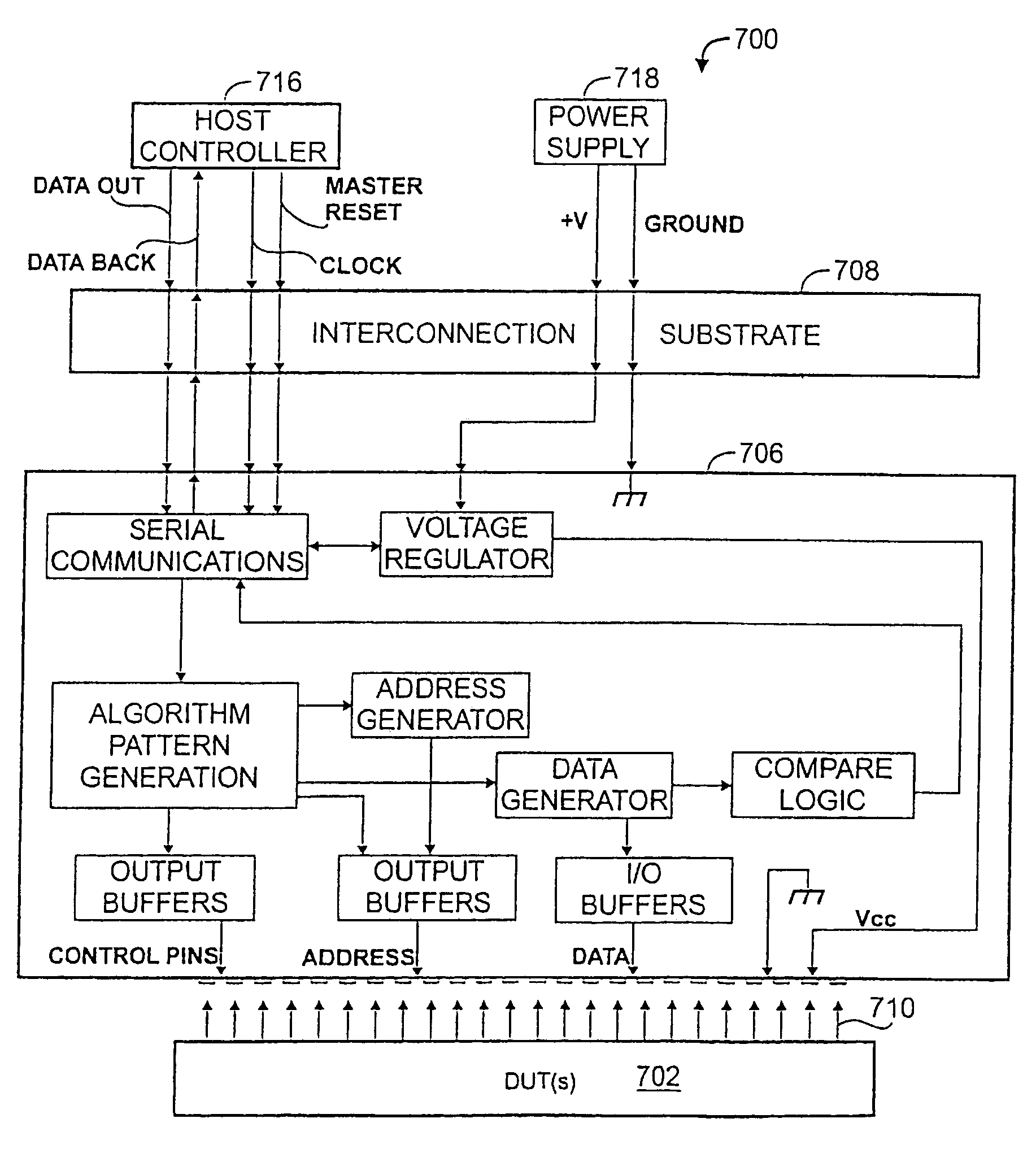
[0054]An advantage of the invention is that DUT operation can be ascertained over a wide temperature range, from well below room temperature to the maximum temperature allowed by the semiconductor process, all without thermally stressing the ASICs.
[0055]The present invention provides the enabling technology for a full wafer-level assembly process.
Problems solved by technology
Due to defects in the wafer, or to defects in one or more of the processing steps, certain ones of the semiconductor devices will not function as designed, these defects may show up initially or may not be apparent until the device has been in operation for an extended period of time.
Precise alignment is also a non-trivial issue, when dealing with spacings (pitch) between adjacent pads as close as 4 mils.
As mentioned hereinabove, this may require many tens of thousands of such contact elements and extremely complex interconnection substrates.
Method used
Image
Click on the blue label to locate the original text in one second.
Reading with bidirectional positioning of images and text.
Examples
Embodiment Construction
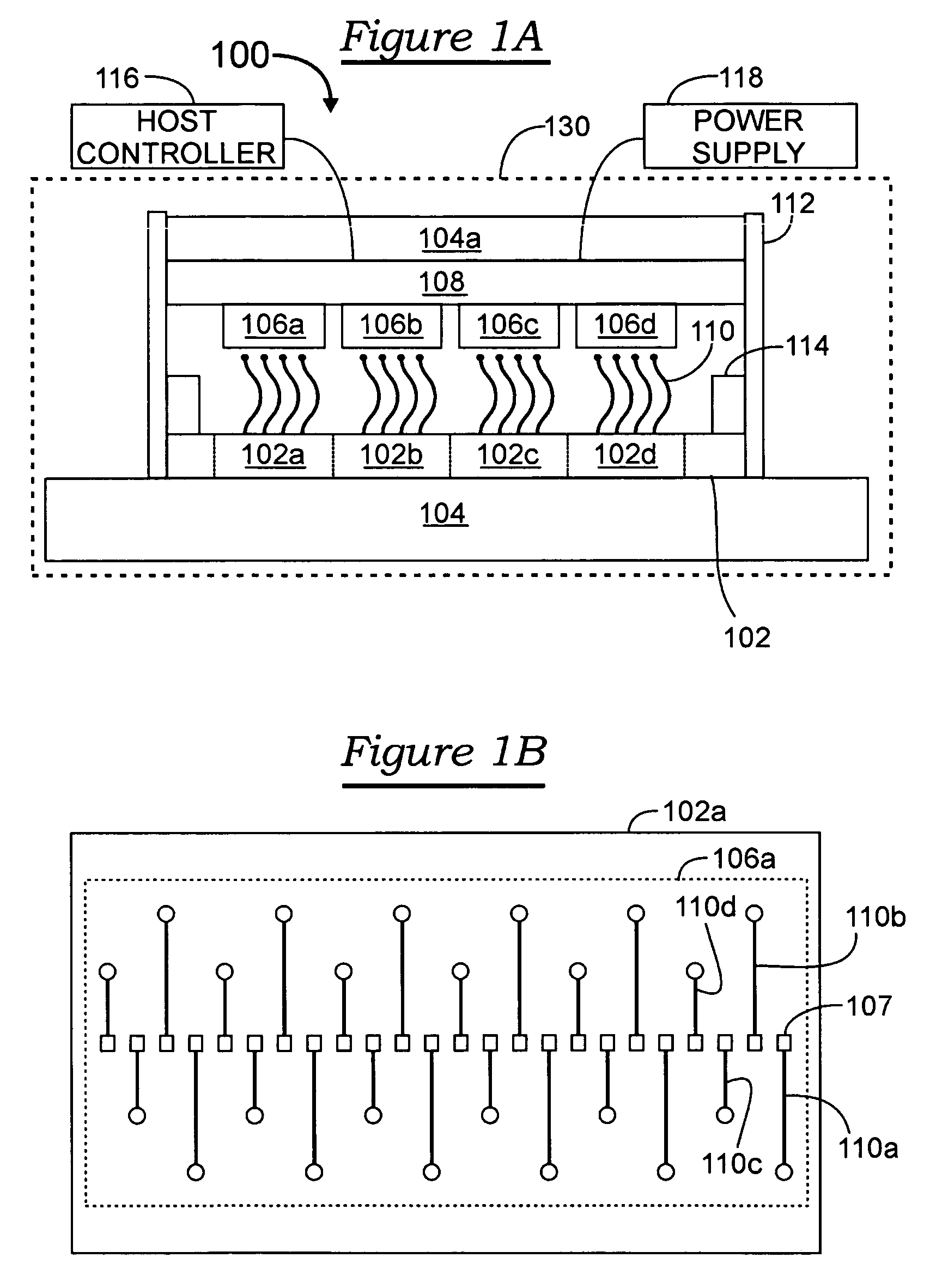
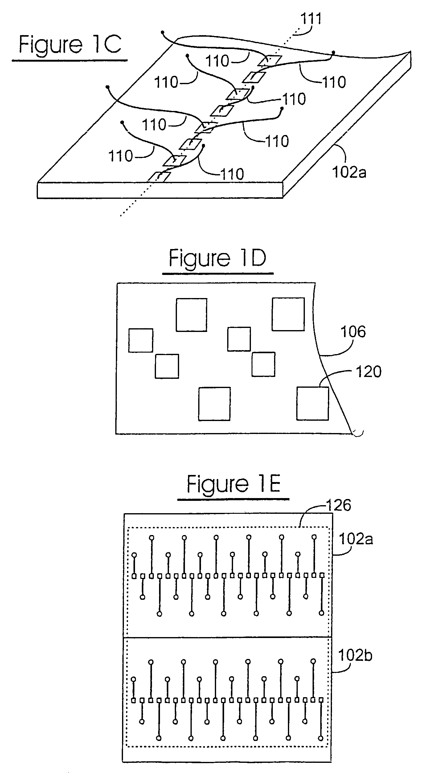
[0073]FIG. 1A illustrates an apparatus 100 for performing a method of wafer-level burn-in and test, according to the invention. A wafer under test (WUT) 102 is disposed (received) on a suitable support, such as a temperature-controlled vacuum chuck 104, such that the semiconductor devices 102a, 102b, 102c, 102d formed on the WUT (the WUT is generally referred to herein as element 102) are facing up (as viewed).
[0074]A plurality (four of many shown) of relatively small active electronic components 106a, 106b, 106c and 106d, such as application-specific integrated circuits (ASICs; referred to generally as element 106) are mounted to a relatively large interconnection substrate (base plate) 108 which is generally of the same size (i.e., diameter) as the WUT 102. For example, the interconnection substrate 108 and the WUT 102 are both eight or twelve inches in diameter. Together, the electronic components (ASICs) 106 and the interconnection substrate 108 constitute a “test substrate”.
[00...
PUM
Abstract
Techniques for performing wafer-level burn-in and test of semiconductor devices include a test substrate having active electronic components such as ASICs mounted to an interconnection substrate or incorporated therein, metallic spring contact elements effecting interconnections between the ASICs and a plurality of devices-under-test (DUTs) on a wafer-under-test (WUT), all disposed in a vacuum vessel so that the ASICs can be operated at temperatures independent from and significantly lower than the burn-in temperature of the DUTs. The spring contact elements may be mounted to either the DUTs or to the ASICs, and may fan out to relax tolerance constraints on aligning and interconnecting the ASICs and the DUTs. Physical alignment techniques are also described.
Description
CROSS-REFERENCE TO RELATED APPLICATIONS[0001]This application is a continuation of U.S. patent application Ser. No. 10 / 326,423 filed on 19 Dec. 2000, now U.S. Pat. Ser. No. 6,788,094, which is a continuation of U.S. patent application Ser. No. 09 / 573,489 filed on 16 May 2000, now U.S. Pat. No. 6,525,555, which is a continuation of U.S. patent application Ser. No. 08 / 784,862, now U.S. Pat. No. 6,064,213 and which is a continuation-in-part of commonly-owned, U.S. patent application Ser. No. 08 / 452,255, now U.S. Pat. No. 6,336,269, (hereinafter “PARENT CASE”) filed 26 May 95 and its counterpart PCT patent application number US95 / 14909 filed 13 Nov. 95, both of which are continuations-in-part of commonly-owned, U.S. patent application Ser. No. 08 / 340,144 filed 15 Nov. 94 now U.S. Pat. No. 5,917,707, and its counterpart PCT patent application number US94 / 13373 filed 16 Nov. 94, both of which are continuations-in-part of commonly-owned, U.S. patent application Ser. 08 / 784,862 filed on 15 ...
Claims
Application Information
Patent Timeline
Application Date:The date an application was filed.
Publication Date:The date a patent or application was officially published.
First Publication Date:The earliest publication date of a patent with the same application number.
Issue Date:Publication date of the patent grant document.
PCT Entry Date:The Entry date of PCT National Phase.
Estimated Expiry Date:The statutory expiry date of a patent right according to the Patent Law, and it is the longest term of protection that the patent right can achieve without the termination of the patent right due to other reasons(Term extension factor has been taken into account ).
Invalid Date:Actual expiry date is based on effective date or publication date of legal transaction data of invalid patent.

