Luminous element and method for preparation thereof

a technology of electroluminescent elements and luminous elements, applied in the direction of discharge tube luminescnet screens, other domestic articles, natural mineral layered products, etc., can solve the problems of narrow viewing angle, insufficient properties, and low response speed

Inactive Publication Date: 2006-08-01
JOLED INC
View PDF18 Cites 13 Cited by
  • Summary
  • Abstract
  • Description
  • Claims
  • Application Information

AI Technical Summary

Problems solved by technology

Recently, among flat-panel-type display devices, liquid crystal display (LCD) panels are used widely, but they still have problems such as a low response speed, a narrow viewing angle, etc., and most of improved versions of these also have problems such as insufficient properties and high costs of panels.
Many studies have been made about such an organic EL element, but the emission efficiency thereof generally has been low and they have been far from practical application in a light-emitting element.
Generally, it is almost impossible to obtain organic compounds that have excellent electron transport capability, and relatively limited compounds can be used for forming the lamination configuration of “hole-transport layer / electron-transport light-emitting layer”.
However, it still has not been possible to obtain those with sufficient characteristics regarding the emission efficiency and lifetime.
In particular, it is said that in the case where a fluorescent material is used, only 25% of an excited state generated by recombination of an electron and a hole contributes to light emission, and this has been a significant problem in pursuing a further improved efficiency.
However, fac tris(2-phenylpyridine)iridium [abbreviated as “Ir(ppy)3”] disclosed in the foregoing thesis and many other heavy metal complexes cannot necessarily be synthesized or purified easily.
On the other hand, a layer made of a single material does not have a sufficient charge transport capability, and exhibits significant concentration quenching (the decrease of the emission intensity at or above a certain concentration).
Therefore, it has been usual to use a charge transport host material doped with a heavy metal complex at an appropriate concentration, but the efficiency and the lifetime depend on the dopant concentration, thereby causing disadvantages in the production.

Method used


Image

  • Luminous element and method for preparation thereof
  • Luminous element and method for preparation thereof
  • Luminous element and method for preparation thereof

Examples


example 1

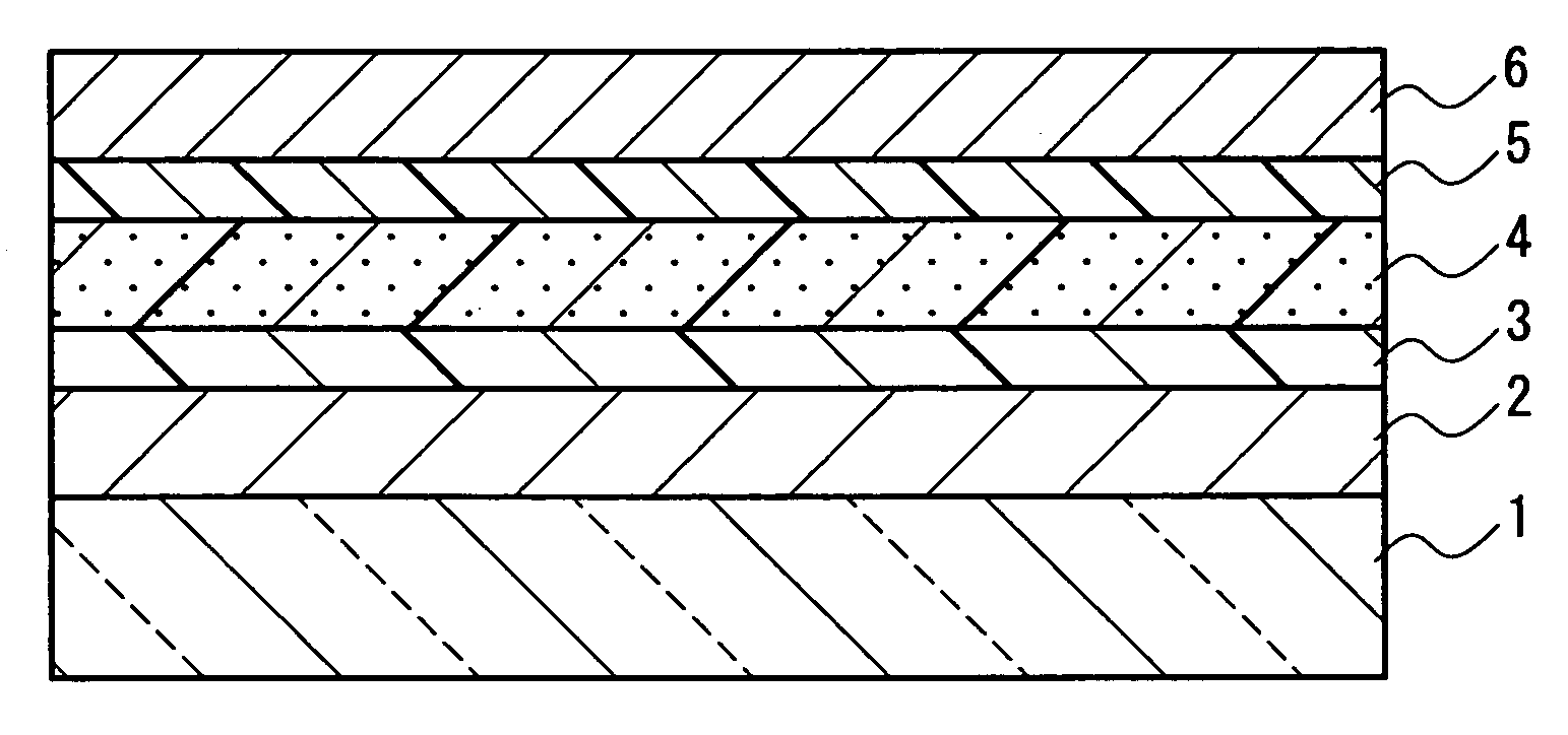
[0110]FIG. 1 is a schematic cross-sectional view illustrating an organic thin film electroluminescent element as a light-emitting element of the present invention. In FIG. 1, 1 denotes a transparent substrate. 2 denotes a hole-injection electrode. 3 denotes a hole-transport layer. 4 denotes a hole-transport light-emitting layer that corresponds to a light-emitting region in the present invention, that contains a compound capable of sustaining the charge transport and a heavy metal so that the heavy metal is co-present as a mixed material. 5 denotes an electron-transport layer. 6 denotes a cathode. Light-emitting elements of the other examples are substantially similar to this embodiment, but the present invention is not limited to the embodiment shown in the drawing.

[0111]The following describes the light-emitting element of the foregoing embodiment in more detail. A commercially-available ITO-applied glass substrate (produced by Sanyo Vacuum Industries Co., Ltd., size: 100 mm×100 m...

example 2

[0134]A thin film EL element sample was produced in the same manner as that of Example 1 except that in forming the hole-transport light-emitting layer of Example 1,[0135][4-(2,2-diphenylvinyl)phenyl](4-methoxyphenyl){4-[(4-methoxyphenyl)phenylamino]phenyl}amine (abbreviated as “M2PPDA-PS”) was used in place of [4-(2,2-diphenylvinyl)phenyl][4-(diphenylamino)phenyl]phenylamine (PPDA-PS).

[0136]Here,[0137][4-(2,2-diphenylvinyl)phenyl](4-methoxyphenyl){4-[(4-methoxyphenyl)phenylamino]phenyl}amine (M2PPDA-PS) was obtained by synthesis as follows.

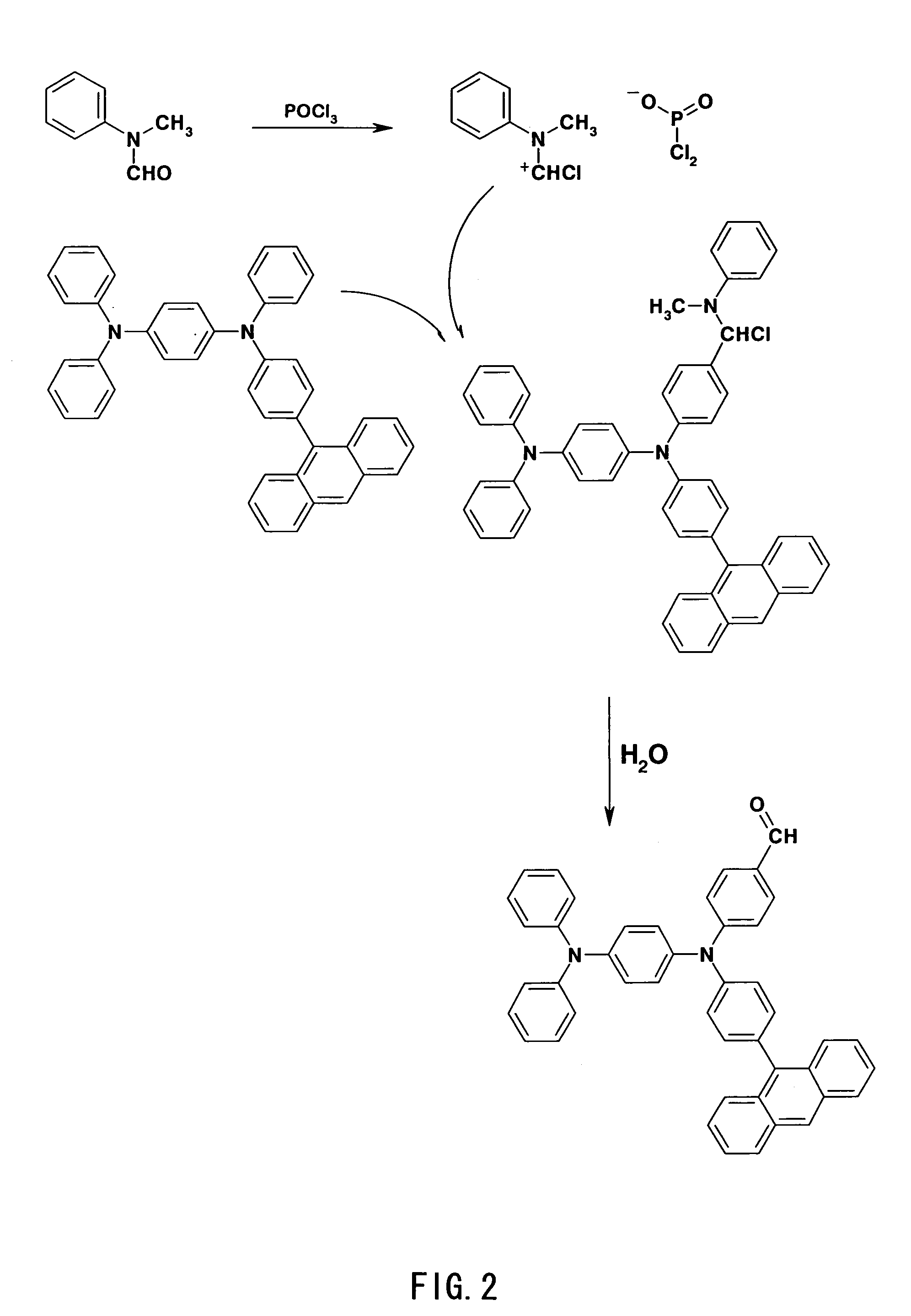
[0138]27.6 g of N,N′-diphenyl-p-phenylenediamine, 50 g of p-iodoanisole, 75 ml of nitrobenzene, 30 g of K2CO3, 7.2 g of copper powder, and I2 (trace) were put in a four-neck flask of 300-milliliter volume, and were refluxed gently over 24 hours by stirring the same while removing generated water by distillation. Subsequently, steam distillation was carried out, and when a distillate no longer came out, residues were extracted using toluene after ...

example 3

[0147]A thin film EL element sample was produced in the same manner as that of Example 1 except that in forming the hole-transport light-emitting layer of Example 1,[0148](4-{[4-(2,2-diphenylvinyl)phenyl](4-(9-anthryl)phenyl)amino}phenyl)diphenylamine (abbreviated as “PPDA-PS-A”) was used in place of[0149][4-(2,2-diphenylvinyl)phenyl][4-(diphenylamino)phenyl]phenylamine (PPDA-PS), and it was co-deposited together with Ir in the same manner as that of Example 1. The same evaluating operations were carried out as those in Example 1 described above. The evaluation results are shown in Table 1.

[0150]Here,[0151](4-{[4-(2,2-diphenylvinyl)phenyl](4-(9-anthryl)phenyl)amino}phenyl)diphenylamine (PPDA-PS-A) was obtained by synthesis as follows.

[0152]After carrying out an Ullmann reaction of N-acetyl-1,4-phenylenediamine as a starting material with iodobenzene, a reaction product was subjected to hydrolysis, and further subjected to an Ullmann reaction with 9-(4-iodophenyl)anthracene, so that ...


PUM

PropertyMeasurementUnit
atomic numberaaaaaaaaaa
thicknessaaaaaaaaaa
thicknessaaaaaaaaaa

Abstract

A light-emitting element having at least a light-emitting region arranged between a pair of electrodes is provided, in which the light-emitting region contains either (A) a light-emitting material, a compound capable of sustaining the charge transport, and a heavy metal as a mixture, or (B) a compound that is capable of sustaining the charge transport and that includes both of a portion for contributing to the charge transport and a portion for contributing to the light emission within the compound, and a heavy metal as a mixture. A method for producing the light-emitting element, and a display device in which a plurality of the light-emitting elements are used, are provided also. With the light-emitting element of the present invention, it is possible to provide an organic thin film electroluminescent element that has a high emission efficiency, whose materials are easy to synthesize as compared with a heavy metal complex-doped element that has been studied widely in recent years, that has a small concentration quenching, and that is stable and uniform. Therefore, the light-emitting element of the present invention is applicable as a light source for use in a flat-panel-type self-luminous display device and for other various purposes such as communication and illumination.

Description

TECHNICAL FIELD[0001]The present invention relates to a thin film electroluminescent (EL) element such as, for instance, a self-luminous light-emitting element, which is suitable as a light source for use in a flat-panel-type self-luminous display device and for other various purposes such as communication and illumination. It also relates to a method for producing the same, and to a display device employing the same.BACKGROUND ART[0002]Recently, among flat-panel-type display devices, liquid crystal display (LCD) panels are used widely, but they still have problems such as a low response speed, a narrow viewing angle, etc., and most of improved versions of these also have problems such as insufficient properties and high costs of panels. Among these, thin film EL elements have drawn attention as new expected self-luminous light-emitting elements with excellent visibility and high response speeds, which are expected to be applicable in a wide range of fields. Particularly, various st...

Claims


Application Information

Patent Timeline
Patent Type & Authority Patents(United States)
IPC IPC(8): H05B33/12H01L29/08H01L51/30H01L51/50
CPCH01L51/002H01L51/0052H01L51/0059Y10S428/917H01L51/0084H01L51/5012H01L2251/308H01L51/0081H10K71/30H10K85/615H10K85/631H10K85/324H10K85/341H10K50/11H10K2102/103
Inventor SATOU, TETSUYAMATSUO, MIKIKOSUGIURA, HISANORIUEMURA, TSUYOSHI
Owner JOLED INC
Why Eureka
Try Eureka