Method and system to enhance differential dynamic range and signal/noise in CMOS range finding systems using differential sensors

a technology of differential dynamic range and signal/noise, applied in the field of solid-state optical range finding sensing systems, can solve the problems of inability to accurately determine distance solely and inability to accurately determine distance from the amplitude and brightness of an intensity image, etc., to achieve the effect of improving the resilience to ambient ligh

Active Publication Date: 2007-01-02
MICROSOFT TECH LICENSING LLC
View PDF8 Cites 147 Cited by
  • Summary
  • Abstract
  • Description
  • Claims
  • Application Information

AI Technical Summary

Benefits of technology

[0028]In another embodiment of what is now the '549 patent, the common mode component of the integrated capacitor voltages was reset periodically to prevent either photodiode detector from saturating. However the differential component of the integrated capacitor voltages was preserved. The result was to extend effective differential dynamic range of the differential sensor in the presence of ambient light by avoiding the effects of saturation.
[0029]In parent co-pending application Ser. No. 11 / 110,982 filed 19 Apr. 2005, further improvements are described for differential pixels, e.g., the circuitry associated with each pixel differential photodetector. More specifically, the '982 application describes pixels with improved common mode rejection, and improved retention of the desired differential signal component, accompanied by acceptably low KT / C noise due to capacitance. In one embodiment, signals to the pixel photodetector differential inputs are coupled as input to an operational amplifier and to a differential signal capacitor, configured as an integrator. During integration, charge from the detectors is accumulated in their integration capacitors. During a charge dump operation, at least half the total differential detection signal charge from the integration capacitors is read into at least one differential signal capacitor. Such charge dumping periodically transfers the differential detector signal into the differential signal capacitor(s) for storage. Thus during common mode resets, which usually follow dump operations, the differential detection signal on the integration capacitor is essentially zero, thus reducing the chance of differential charge loss. The desired result is enhanced common mode rejection with relatively little loss in differential detection signal.
[0031]Further embodiments of the present invention enhance differential pixel signal / noise ratio by dynamically maximizing gain on the operational amplifier associated with each differential pixel. Because such operational amplifiers are found early in the detection signal paths, high amplifier gain (AG) reduces effective noise contribution downstream in the signal path by 1 / Ag. Gain of each such amplifier is variably controlled to adjust AG individually for each pixel as a function of its present signal value. Within the array of differential pixels, each amplifier is first operated at maximum AG, and integration capacitor values are readout and stored in a row buffer. AG for each amplifier in the row is then incrementally decreased, and the row buffer is updated only for those amplifiers whose associated integration capacitor is not presently saturated. The above process is repeated until the value in the row buffer corresponds to the highest non-saturating gain for each amplifier associated with the row. The row buffer also records the value of the highest non-saturating gain for each amplifier associated with the pixels in that row. At this juncture the row buffer is readout, and the process is repeated for the next row in the array, and so on continuously. In this fashion amplifier values of AG are individually maximized, commensurate with avoiding overload or saturation of components downstream in the signal path. The desired result is enhanced signal / noise ratio. Alternative embodiments can, of course, increment rather than decrement amplifier gain or even randomly or otherwise scan or vary AG and cause the row buffer to latch the non-saturated gain value for each amplifier associated with pixels in a row.

Problems solved by technology

Unfortunately, it is difficult to accurately determine distance solely from the amplitude and brightness of an intensity image.
The result would be that the more distant, shiny, object is erroneously reported as being closer to the system than the closer, duller, object.
In a range finding system used to control robot machinery in an industrial setting, such errors may be intolerable for reasons of safety to nearby human operators.
Simply stated, two-dimensional intensity-based systems are very prone to measurement error.
As described herein, high levels of ambient light relative to levels of light from energy source 40 can be detrimental to reliable operation of system 10.
Even if ambient light could be measured and subtracted from the total signal, its noise component (e.g., shot noise) would still degrade system performance.
Further, the presence of ambient light can have even more severe consequences by causing the pixel detector to saturate.
However the presence of strong ambient light, sunlight perhaps, can degrade the performance of differential pixel detectors.
But it still remains a challenge to provide a TOF system with differential pixel photodetectors that are protected from saturation, including saturation from differential mode signals, while enhancing signal / noise ratios.
Such detection current signals are too small in magnitude to be measured directly.
Due to the saturation condition, the pixel does not output any useful result in that the differential voltage, which contained range information, is now zero.
Thus, a very real problem with prior differential pixel detectors is that the dynamic range of the pixel is not sufficient to handle strong ambient light.

Method used


Image

  • Method and system to enhance differential dynamic range and signal/noise in CMOS range finding systems using differential sensors
  • Method and system to enhance differential dynamic range and signal/noise in CMOS range finding systems using differential sensors
  • Method and system to enhance differential dynamic range and signal/noise in CMOS range finding systems using differential sensors

Examples


Embodiment Construction

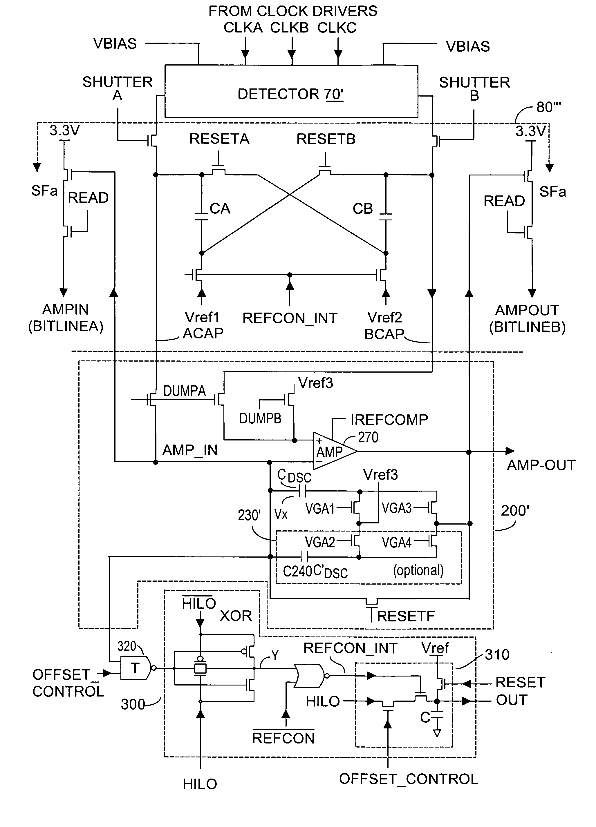
[0072]Before describing the present invention, whose description commences with FIG. 14, it is useful to first describe embodiments of U.S. Pat. No. 6,919,549, from which priority is claimed. Description of the '549 patent will be made with reference to FIGS. 3A–10B. Next a description of priority application Ser. No. 11 / 110,982 will be made with reference to FIGS. 11, 12, and 13. An understanding of the operation of pixel differential photodetectors and the evolution of their associated electronic circuitry (sometimes referred to herein as differential pixel) will now be described with reference to FIGS. 3A–13, to enable a better understanding of the present invention.

[0073]FIG. 3A, taken from the '549 patent, depicts one-half of differential pixel detector 70′, where it is understood that TOF system 100 shown in FIG. 1B might now employ an array 60′ of rows and columns of differential pixel detectors 70′ as will now be described, rather than pixel detectors 70. In FIG. 3A, only on...


PUM


Abstract

Dynamic range of a differential pixel is enhanced by injecting, synchronously or asynchronously, a fixed compensating offset (ΔV) into a differential signal capacitor whenever magnitude of the differential signal across the capacitor exceeds a predetermined value. The number (N) of ΔV offsets made is counted. Effective differential signal capacitor voltage V(t)=Vo+N·ΔV, where Vo is capacitor voltage. Differential pixel signal / noise ratio is increased by dynamically maximizing operational amplifier gain AG for each differential pixel.

Description

CROSS-REFERENCES TO RELATED APPLICATIONS[0001]Priority is claimed from co-pending U.S. provisional patent application No. 60 / 650,900 filed 8 Feb. 2005 entitled Improved Op Amp Assisted CMR, No. 60 / 650,901 filed 8 Feb. 2005 entitled High Active Light Dynamic Range for 3-D Imaging, and No. 60 / 650,902 filed 8 Feb. 2005 entitled A Postiori VGA Gain Setting. Further, this is a continuation-in-part from co-pending U.S. patent application Ser. No. 11 / 110,982 filed 19 Apr. 2005, entitled Method and System to Differentially Enhance Sensor Dynamic Range Using Enhanced Common Mode Reset, which application was a continuation in-part of U.S. utility application entitled Method and System to Differentially Enhance Sensor Dynamic Range, application Ser. No. 10 / 823,415, filed 12 Apr. 2004, now U.S. Pat. No. 6,919,549 (2005) Method and System to Differentially Enhance Sensor Dynamic Range.FIELD OF THE INVENTION[0002]The invention relates generally to solid state optical range finding sensing systems...

Claims


Application Information

Patent Timeline
Patent Type & Authority Patents(United States)
IPC IPC(8): H01L27/00
CPCG01C3/06G01S7/487G01S17/08G01S7/4868H04N5/3745G01S17/89G01S7/4863H04N5/35536G01S17/894H04N25/58H04N25/77
Inventor BAMJI, CYRUSSALAMA, KHALED
Owner MICROSOFT TECH LICENSING LLC
Why Eureka
Try Eureka