Programming inhibit for non-volatile memory

a non-volatile memory, programming inhibit technology, applied in static storage, digital storage, instruments, etc., can solve the problems of unprogrammed cells, unselected cells connected to the word line, inadvertent programming, etc., to reduce or avoid program disturb

Active Publication Date: 2007-01-30
SANDISK TECH LLC
View PDF30 Cites 49 Cited by
  • Summary
  • Abstract
  • Description
  • Claims
  • Application Information

AI Technical Summary

Benefits of technology

[0020]The present invention, roughly described, pertains to technology for programming memory devices in a manner that reduces or avoids program disturb. In accordance with one embodiment, the storage elements of a NAND string are partitioned into at least two regions. A first boosting voltage is applied to the first region of the string while a second larger boosting voltage is applied to the second region. The first region includes the addressed row or selected word line for programming. The first and second boosting voltages are applied to all the NAND strings of a targeted block while inhibiting all of the NAND strings from being programmed, independent of the data to be programmed. In this manner, the second boosting voltage can be made larger without inducing program disturb on the memory cells receiving the larger boosting voltage. The channel of a NAND string will be boosted to a voltage potential that is a result of capacitive coupling between the first boosting voltage and the second boosting voltage. The boosted voltage potentials of the NAND string channels are then trapped within all or part of the first region by lowering the boosting voltage on one or more bounding rows (in one embodiment). The second boosting voltage is then lowered and data is applied to the bit lines of the NAND strings to select the appropriate strings for programming (e.g., by taking the selected string bit lines to 0 volts). In this way, the trapped voltage potential discharges from NAND strings selected for programming, while remaining in the boosted state during programming for NAND strings including a storage element to be inhibited.
[0021]In one embodiment, a method of programming non-volatile memory includes boosting a voltage potential of a channel of a first group of non-volatile storage elements, trapping at least a portion of the voltage potential in a region of the channel associated with a first subset of the first group of non-volatile storage elements, and enabling programming of a second group of non-volatile storage elements subsequent to trapping the voltage potential. Boosting the voltage potential can include applying a first boosting voltage to the first subset of the first group and applying a second boosting voltage to a second subset of the first group. The second boosting voltage can be lowered after trapping the voltage potential but prior to enabling programming to the second group of non-volatile storage elements so as to avoid off-row program disturb from a large second boosting voltage. Accordingly, the second boosting voltage can be of a size that may normally cause programming of a memory cell of a string having its bit line biased for programming. In one embodiment, programming of the first group and the second group is inhibited while the second boosting voltage is applied. In one embodiment, the voltage potential is trapped in a region of the channel associated with the first subset of storage elements by lowering the boosting voltage on one or more word lines that bound the first subset.

Problems solved by technology

A problem arises when it's desired to program one cell on a word line without programming other cells connected to the same word line, for example, when it's desired to program cell 224 and not cell 244.
Because the program voltage is applied to all cells connected to a word line, an unselected cell (a cell that is not to be programmed) connected to the word line, especially a cell adjacent to the cell selected for programming, may become inadvertently programmed.
Because of this negative charge on the floating gates, the boosting potential doesn't get high enough and there still may be program disturb on the last few word lines.
If Vpass is too low, boosting in the channel is insufficient to prevent program disturb.
While LSB and EASB provide an improvement over self boosting, they also present a problem that depends on whether the source side neighbor cell (cell 246 is the source side neighbor of cell 244) is programmed or erased.
GIDL will cause the boosted voltage to leak away prematurely, resulting in a programming error.
If the leakage current is high enough, the boosting potential in the channel region will go down and there can be program disturb.
Thus, the voltage in the boosted junction will drop quickly, causing program disturb.
Rather that string is operating in self boosting mode, and self boosting mode has the problems discussed above.
This scenario is most likely if other source side cells are programmed, which limits source side boosting.
This issue is most problematic with shorter channel lengths.
In addition to the identified problems of each of the aforementioned prior art techniques for reducing or preventing program disturb, the amount of pass or boosting voltage that is applied to unselected world lines has an upper and lower limit.
If the pass voltage is below a certain level, insufficient boosting of the channel will occur and programming of an addressed memory cell that is to be fully inhibited can occur.

Method used


Image

  • Programming inhibit for non-volatile memory
  • Programming inhibit for non-volatile memory
  • Programming inhibit for non-volatile memory

Examples


Embodiment Construction

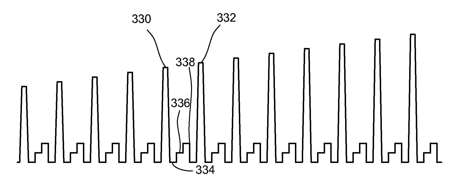
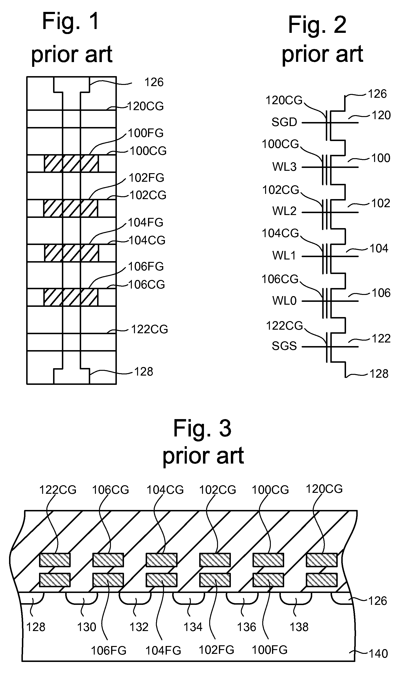
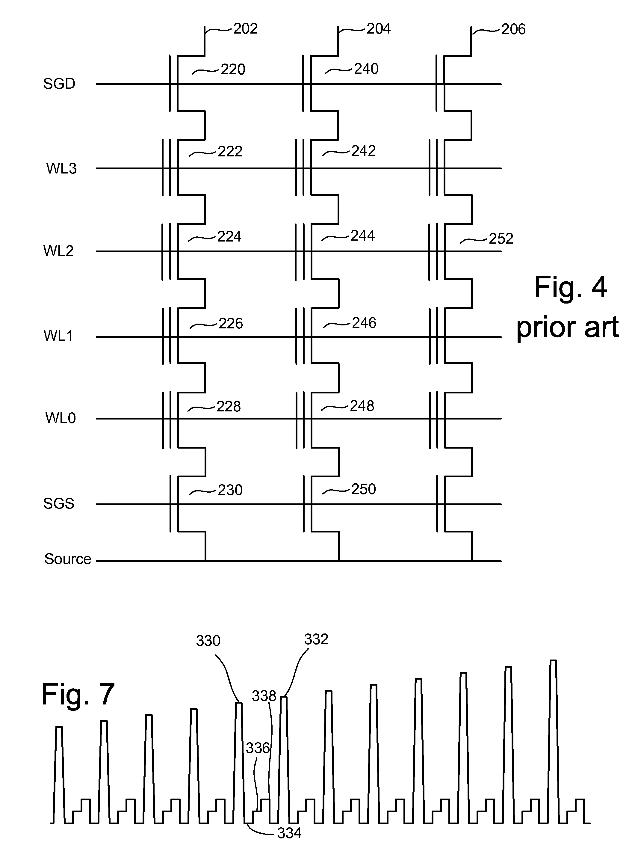
[0041]The invention is illustrated by way of example and not by way of limitation in the figures of the accompanying drawings in which like references indicate similar elements. It should be noted that references to an or one embodiment in this disclosure are not necessarily to the same embodiment, and such references mean at least one.

[0042]In the following description, various aspects of the present invention will be described. However, it will be apparent to those skilled in the art that the present invention may be practiced with only some or all aspects of the present disclosure. For purposes of explanation, specific numbers, materials, and configurations are set forth in order to provide a thorough understanding of the present invention. However, it will be apparent to one skilled in the art that the present invention may be practiced without the specific details. In other instances, well-known features are omitted or simplified in order not to obscure the present invention.

[0...


PUM


Abstract

A non-volatile memory system is programmed so as to reduce or avoid program disturb. In accordance with one embodiment, the storage elements of a NAND string are partitioned into at least two regions. A first boosting voltage is applied to the first region of the string while a second larger boosting voltage is applied to the second region. The first region includes the addressed row or selected word line for programming. The boosting voltages are applied to the NAND strings of a block while the NAND strings are being inhibited from programming. In this manner, the second boosting voltage can be made larger without inducing program disturb on the memory cells receiving the larger boosting voltage. The boosted voltage potentials of the NAND string channels are trapped within the first region by lowering the boosting voltage on one or more bounding rows. The second boosting voltage is then lowered and data is applied to the bit lines of the NAND strings to select the appropriate strings for programming. The trapped voltage potential discharges or remains in the boosted state for programming depending on whether a string is selected for programming or is to remain inhibited from programming.

Description

BACKGROUND OF THE INVENTION[0001]1. Field of the Invention[0002]The present invention relates generally to technology for programming non-volatile memory devices.[0003]2. Description of the Related Art[0004]Semiconductor memory devices have become more popular for use in various electronic devices. For example, non-volatile semiconductor memory is used in cellular telephones, digital cameras, personal digital assistants, mobile computing devices, non-mobile computing devices and other devices. Electrical Erasable Programmable Read Only Memory (EEPROM) and flash memory are among the most popular non-volatile semiconductor memories.[0005]One example of a flash memory system uses the NAND structure, which includes arranging multiple transistors in series, sandwiched between two select gates. The transistors in series and the select gates are referred to as a NAND string. FIG. 1 is a top view showing one NAND string. FIG. 2 is an equivalent circuit thereof. The NAND string depicted in F...

Claims


Application Information

Patent Timeline
Patent Type & Authority Patents(United States)
IPC IPC(8): G11C11/34G11C16/04G11C16/12
CPCG11C16/12
Inventor GUTERMAN, DANIEL C.
Owner SANDISK TECH LLC
Why Eureka
Try Eureka