Modular connector assembly with adjustable distance between contact wafers

a module connector and contact wafer technology, applied in the direction of coupling devices, two-part coupling devices, electrical devices, etc., can solve the problems of labor intensive, slow manufacturing and assembly process, and high cos

Inactive Publication Date: 2007-03-27
TE CONNECTIVITY CORP
View PDF4 Cites 51 Cited by
  • Summary
  • Abstract
  • Description
  • Claims
  • Application Information

AI Technical Summary

Benefits of technology

[0007]In another aspect, an electrical connector is provided that includes a housing having a mating end and a loading end. First and second contact wafers are loaded into the loading end of the housing. The first and second contact wafers each have a dielectric carrier holding a contact therein. The carriers have outer walls. A wafer spacer is configured to be positioned between the first and second contact wafers in one of different first and second orientations relative to the outer walls of the first and second contact wafers. The wafer spacer has opposed first and second side walls that are separated by a spacer core thickness. The first side wall has first and second...

Problems solved by technology

The manufacturing and assembly proce...

Method used


Image

  • Modular connector assembly with adjustable distance between contact wafers
  • Modular connector assembly with adjustable distance between contact wafers
  • Modular connector assembly with adjustable distance between contact wafers

Examples


Embodiment Construction

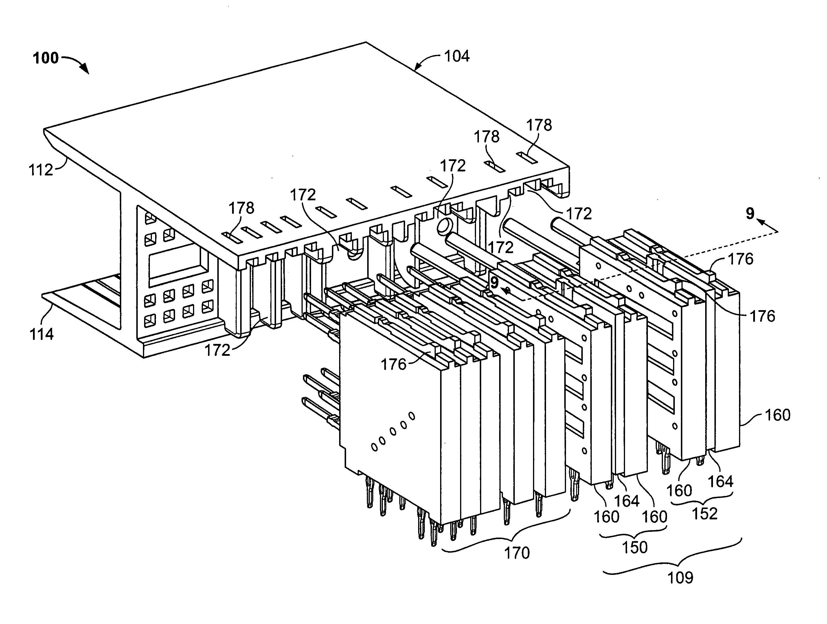
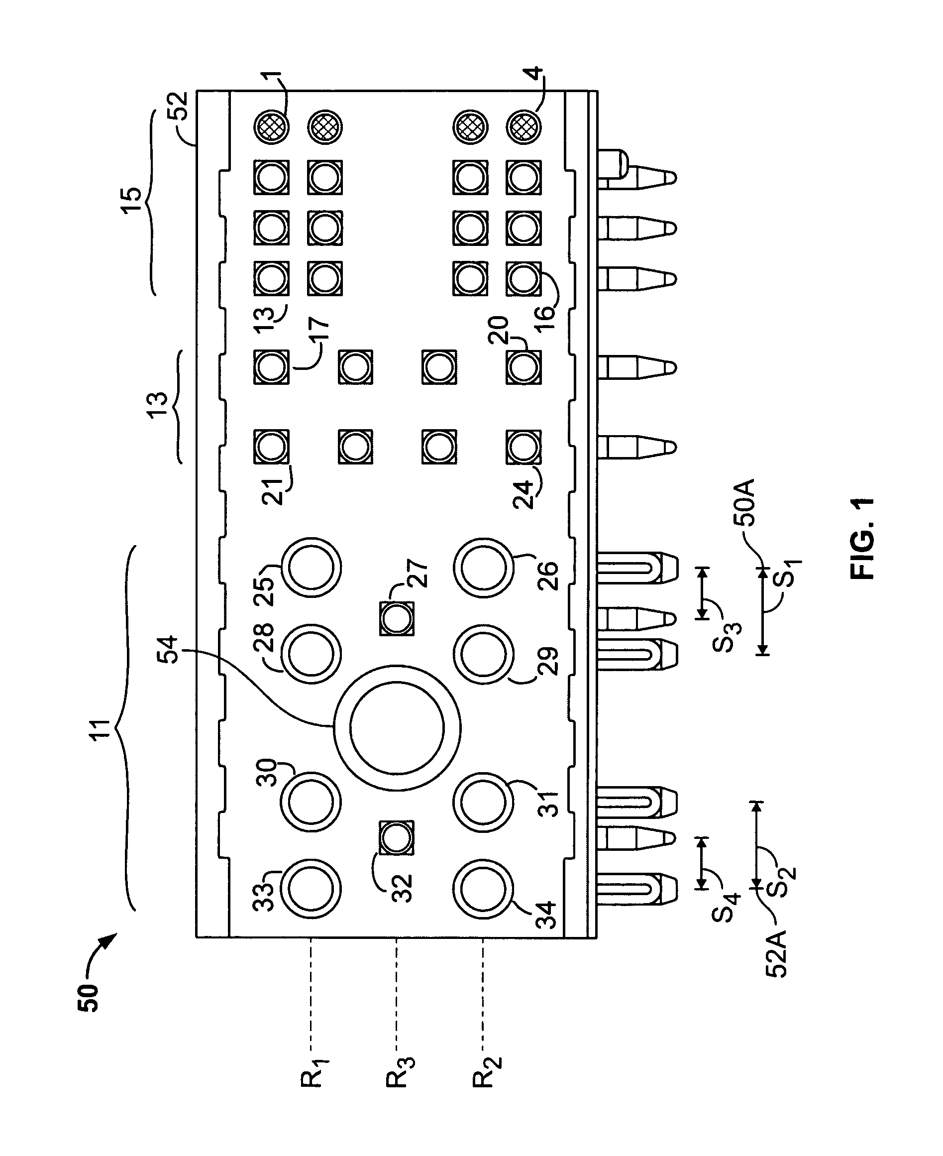
[0018]FIG. 1 illustrates a front elevational view of an Advanced Telecom Computing Architecture (Advanced TCA) zone #1 compliant connector 50 formed in accordance with an embodiment of the present invention. The connector 50 includes a main housing body 52 having a guide post 54. The connector 50 is divided into a power delivery portion or zone 11, a first signal delivery portion or zone 13 and a second signal delivery portion or zone 15. Power and signal contacts are numbered one to thirty four starting at the upper right corner of the main housing body 12 and sequentially moving down each column. On each side of the guide post 54, the power delivery portion of the connector 50 includes an array of four power contacts with an inter-nested signal contact. Power contacts 25, 26, 28, and 29 are provided with an inter-nested signal contact 27. Power contacts 25 and 26 are vertically aligned with one another and power contacts 28 and 29 are similarly vertically aligned with one another....


PUM


Abstract

An electrical connector includes a housing having a mating end and a loading end. First and second contact wafers are loaded into the loading end of the housing. The first and second contact wafers each have a dielectric carrier holding a contact therein. The carriers have outer walls, wherein at least one of the outer walls on each of the carriers has a spacer engagement element provided thereon. A wafer spacer is configured to be positioned between the first and second contact wafers. The wafer spacer is positioned in one of different first and second orientations relative to the side walls of the first and second contact wafers. The wafer spacer has opposed first and second side walls that are separated by a spacer core thickness. The first side wall has a wafer engagement element provided thereon. When the wafer spacer is in the first orientation, the wafer spacer separates the first and second contact wafers by a first distance. When the wafer spacer is in the second orientation, the wafer spacer separates the first and second contact wafers by a second distance that is greater than the first distance.

Description

BACKGROUND OF THE INVENTION[0001]The invention relates generally to electrical connectors and more particularly to a connector having contact wafers that are separated by an adjustable distance.[0002]Numerous connectors exist for joining signal and power lines between a backplane and a daughter board. Industry standards are often developed to standardize or define certain aspects of board-to-board interfaces. One such standard is the Advanced Telecom Computing Architecture (Advanced TCA) which defines several physical and electrical characteristics. For example, the backplane is divided into zones with zone #1 being defined for power and management, zone #2 for data transport, and zone #3 being user defined rear I / O. Typically, in Advanced TCA compliant communications equipment, the backplane has multiple locations for contacts to plug into receptacles on the backplane. Typically, the connector forms a right angle connector.[0003]The connector may include contacts having a combinati...

Claims


Application Information

Patent Timeline
IPC IPC(8): H01R13/58
CPCH01R13/518H01R23/688H01R12/727H01R13/6585
Inventor MCALONIS, MATTHEW RICHARDTAYLOR, ATTALEE S.HAMNER, RICHARD ELOF
Owner TE CONNECTIVITY CORP
Why Eureka
Try Eureka