Chip resistor

a chip resistor and resistor technology, applied in the direction of sustainable manufacturing/processing, final product manufacturing, semiconductor/solid-state device details, etc., can solve the problems of increasing the density and complexity of the wiring pattern increasing the cost of multi-layered printed wiring boards with a number of layers, and difficulty in reducing the size or increasing the density of the printed wiring board

Inactive Publication Date: 2007-10-02
KK TOSHIBA
View PDF6 Cites 5 Cited by
  • Summary
  • Abstract
  • Description
  • Claims
  • Application Information

AI Technical Summary

Problems solved by technology

In accordance with these advances, the wiring patterns of the printed wiring boards in which circuits with desired functions are becoming more dense and complicated.
However, multi-layered printed wiring boards with a number of layers are costly.
However, a jumper wire takes up an excessive area of the printed wiring board (, as compared to the case where a jumper wire is provided inside the laminated circuit board of a multi-layered printed wiring board), and therefore it is difficult to reduce the size or increase the density of the printed wiring board.

Method used


Image

  • Chip resistor
  • Chip resistor
  • Chip resistor

Examples


Embodiment Construction

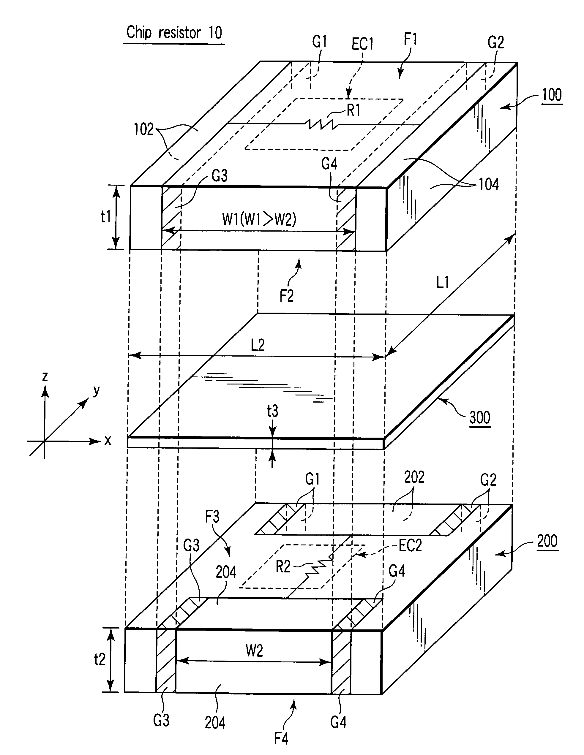
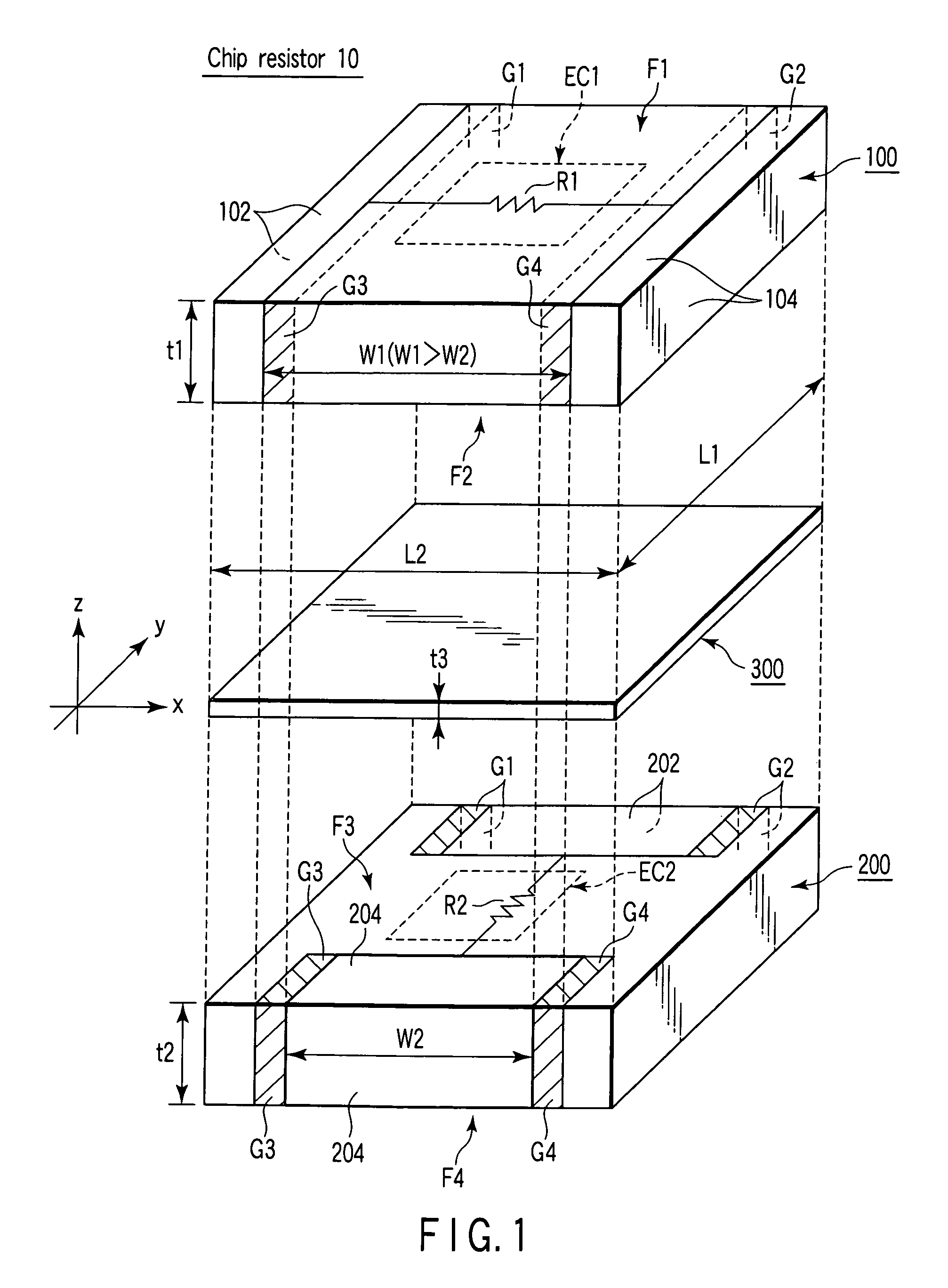
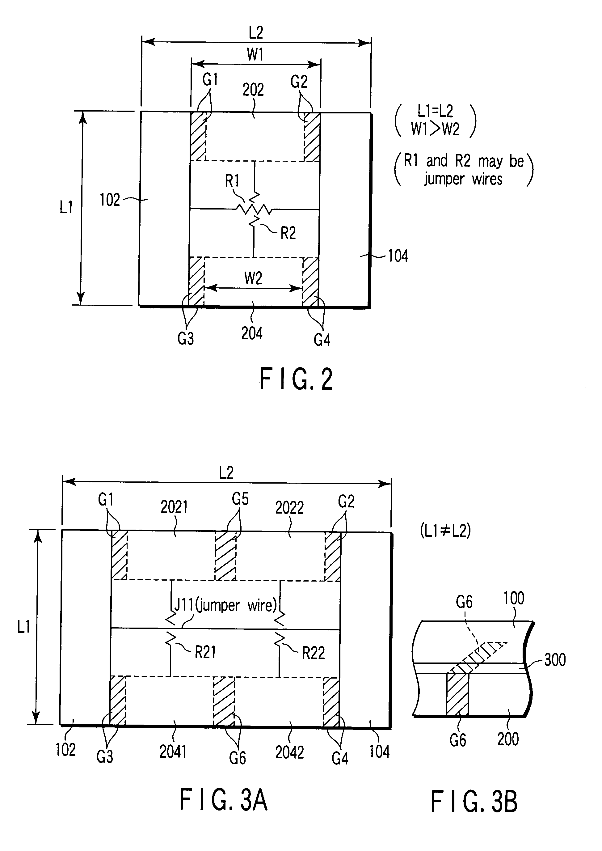
[0016]Various embodiments according to the invention will be described hereinafter with reference to the accompanying drawings. In general, according to one embodiment of the invention, a chip resistor includes a first substrate having a polygonal flat-panel shape, made of an electrical insulating material and having a first upper surface and a first lower surface, a second substrate having a polygonal flat-panel shape, made of an electrical insulating material and having a second upper surface and a second lower surface, and a joint layer interposed between the first lower surface of the first substrate and the second upper surface of the second substrate and made of an electric insulating material, the chip resistor comprises first and second electrodes formed on two first opposing sides of the polygonal flat-panel shape of the first substrate, a first electric circuit formed on the first upper surface and / or the first lower surface between the first electrode and the second elect...


PUM


Abstract

Chip resistor includes the rectangular first substrate made of ceramics and having surfaces, the rectangular second substrate made of ceramics and having surfaces, and a joint layer interposed between the surfaces, and electrodes are formed on two opposing sides of the substrate and resistor is formed between the electrodes. Further, electrodes are formed on two opposing sides of the substrate and resistor is formed between the electrodes.

Description

CROSS-REFERENCE TO RELATED APPLICATIONS[0001]This application is based upon and claims the benefit of priority from Japanese Patent Application No. 2005-346088, filed Nov. 30, 2005, the entire contents of which are incorporated herein by reference.BACKGROUND[0002]1. Field[0003]The present invention relates to a chip resistor to be directly mounted on a wiring pattern of a printed wiring board by, for example, soldering. More specifically, the invention relates to a chip resistor of a multi-layered structure in which a plurality of resist elements and jumper wiring, etc. can be built in to be electrically independently from each other.[0004]2. Description of the Related Art[0005]Recent years, electronic devices are being further advanced in terms of downsizing, density and functions as can be seen in the field of mobile telephones, handy movie cameras, etc. In accordance with these advances, the wiring patterns of the printed wiring boards in which circuits with desired functions are...

Claims


Application Information

Patent Timeline
Patent Type & Authority Patents(United States)
IPC IPC(8): H01C1/012
CPCH01C1/01H01C1/16H01C7/001H01C17/006H05K3/222H01C13/02H05K2201/10636H05K2201/10363Y02P70/50
Inventor YOKOO, HIDEO
Owner KK TOSHIBA
Why Eureka
Try Eureka