High-performance flash memory data transfer

a flash memory and data transfer technology, applied in the field of flash memory devices, can solve the problems of insufficient data transfer time, insufficient data rate to achieve the desired delay time, so as to reduce power consumption and reduce voltage swing

US7345926B2Active Publication Date: 2008-03-18SANDISK TECH LLC
15 Cites 21 Cited by

Patent Information

Authority / Receiving Office
US · United States
Patent Type
Patents(United States)
Current Assignee / Owner
Publication Date
2008-03-18

Smart Images

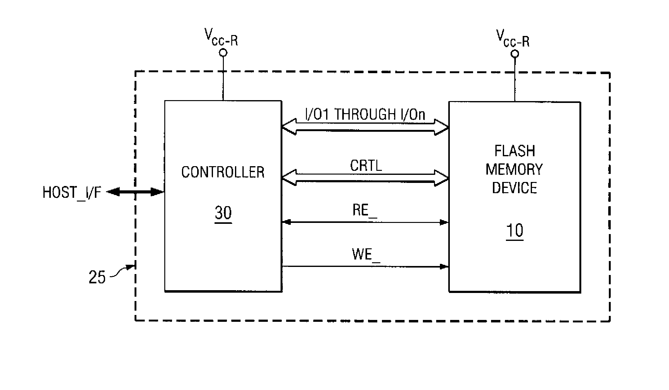
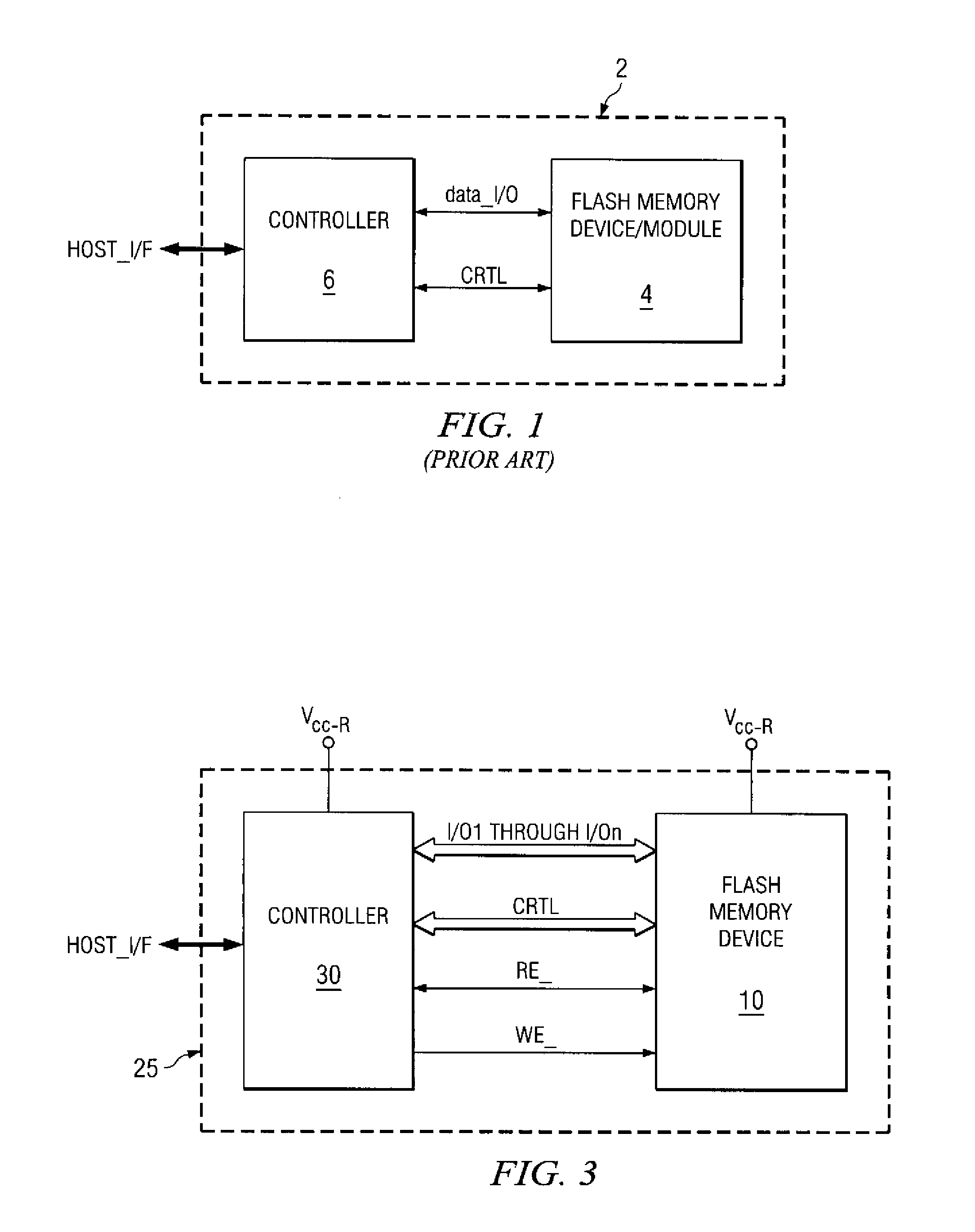
  • Figure 1
    Figure 1
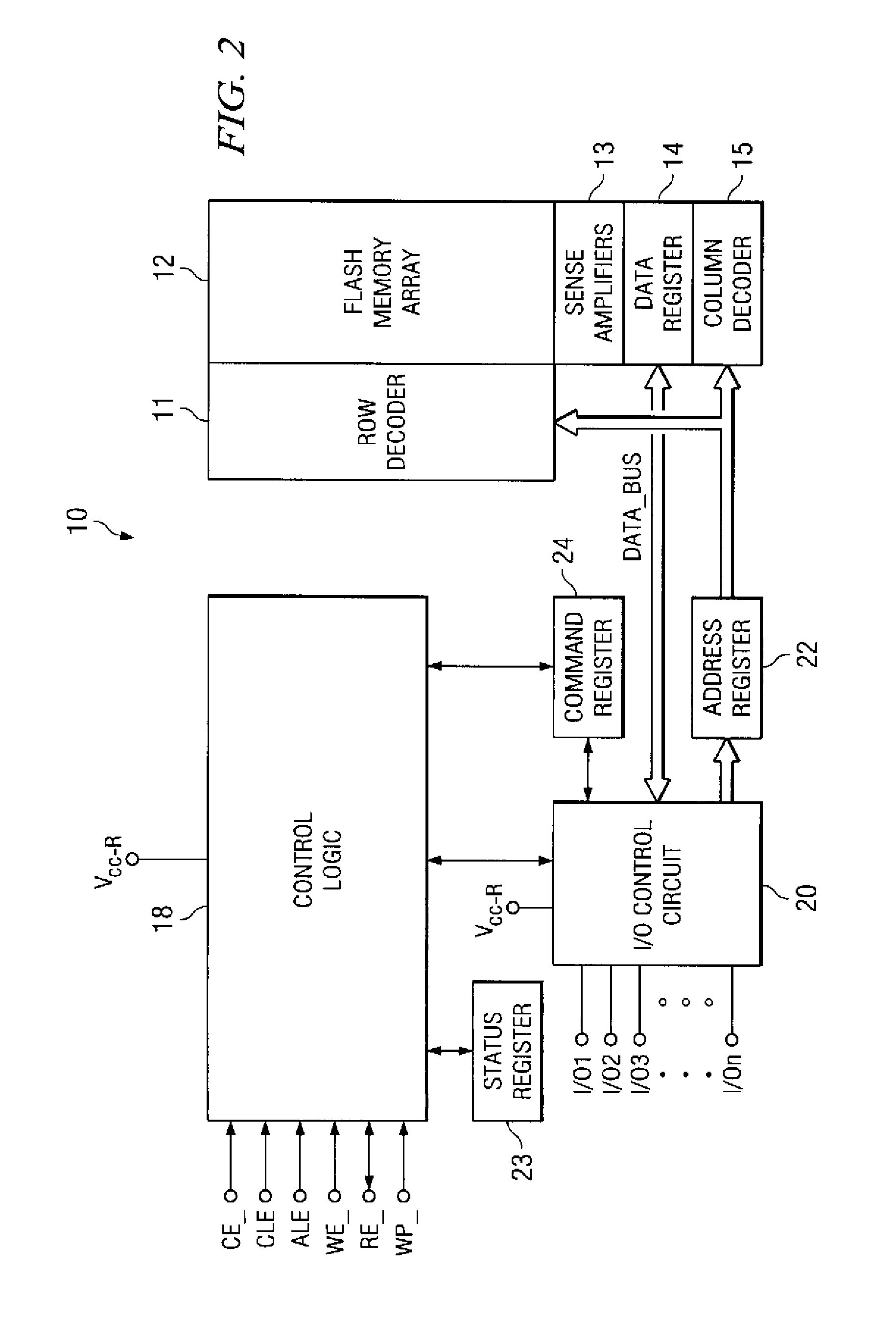
  • Figure 2
    Figure 2
  • Figure 3
    Figure 3
Patent Text Reader

Abstract

A flash memory system including a flash memory device and a controller, operable according to an advanced data transfer mode is disclosed. The flash memory device is operable both in a “legacy” mode, in which read data is presented by the memory synchronously with each cycle of a read data strobe from the controller, and in which input data is latched by the memory synchronously with each cycle of a write data strobe from the controller. In the advanced mode, which can be initiated by the controller forwarding an initiation command to the memory, the flash memory itself sources the read data strobe, and presents data synchronously with both the falling and rising edges of that read data strobe. In the advanced mode, the input data is presented by the controller synchronously with both edges of the write data strobe. The voltage swing of the data and control signals is reduced from conventional standards, to reduce power consumption.
Need to check novelty before this filing date? Find Prior Art

Description

CROSS-REFERENCE TO RELATED APPLICATIONS

[0001] Not applicable.STATEMENT REGARDING FEDERALLY SPONSORED RESEARCH OR DEVELOPMENT

[0002] Not applicable.BACKGROUND OF THE INVENTION

[0003] This invention is in the field of flash memory devices, and is more specifically directed to data communications between flash memory devices and memory controllers in electronic systems.

[0004] As well known in the art, “flash” memories are electrically-erasable semiconductor memory devices that can be erased and rewritten in relatively small blocks, rather than on a chip-wide or large-block basis as in previous electrically-erasable programmable read-only memory (EEPROM) devices. As such, flash memory has become especially popular for applications in which non-volatility (i.e., data retention after removal of power) of the stored data is essential, but in which the frequency of rewriting is relatively low. Examples of popular applications of flash memory include portable audio players, “SIM” card storage of t...

Examples

Embodiment Construction

[0026]The present invention will be described in connection with its preferred embodiment, namely as implemented into a flash memory module, and a subsystem including such a flash memory module, and method of operating the same. More specifically, this exemplary flash memory module is described as a multi-level cell (MLC) flash memory of the NAND type, as it is contemplated that this invention will be particularly useful in connection with such flash memories, in order to enable the use of solid-state non-volatile memory for mass data storage in computer systems. However, it is contemplated that this invention will be useful and beneficial in other applications involving non-volatile solid-state memories of various types. Accordingly, it is to be understood that the following description is provided by way of example only, and is not intended to limit the true scope of this invention as claimed.

[0027]FIG. 2 illustrates an exemplary construction of flash memory device (or module) 10 ...