Eureka AIR delivers breakthrough ideas for toughest innovation challenges, trusted by R&D personnel around the world.

Latch circuit

Inactive Publication Date: 2008-06-17
ALTERA CORP
View PDF3 Cites 7 Cited by
  • Summary
  • Abstract
  • Description
  • Claims
  • Application Information

AI Technical Summary

Benefits of technology

[0010]The pass gate can be controlled to isolate disturbing currents and thereby prevent them from flipping the logic state of the latch circuit. For example, the control signal applied to the pass gates can be −1 Volt or lower when programming the logic circuit and can be raised to about zer

Problems solved by technology

The circuit of FIG. 1 has the disadvantage that it has a relatively high soft error rate (SER).
As a result, this circuit is not an attractive candidate for use in critical memory functions such as memory cells in configuration random access memory (CRAM) where a single erroneous bit in the CRAM may render unusable the programmable logic array (PLA) that is programmed by the CRAM.
However, it is not practical in conventional CMOS technology to achieve significant resistance values in a small layout area.
As a result, feedback resistors are not used in latch circuits for technology nodes less than 0.25 um.

Method used


Image

  • Latch circuit
  • Latch circuit
  • Latch circuit

Examples


Embodiment Construction

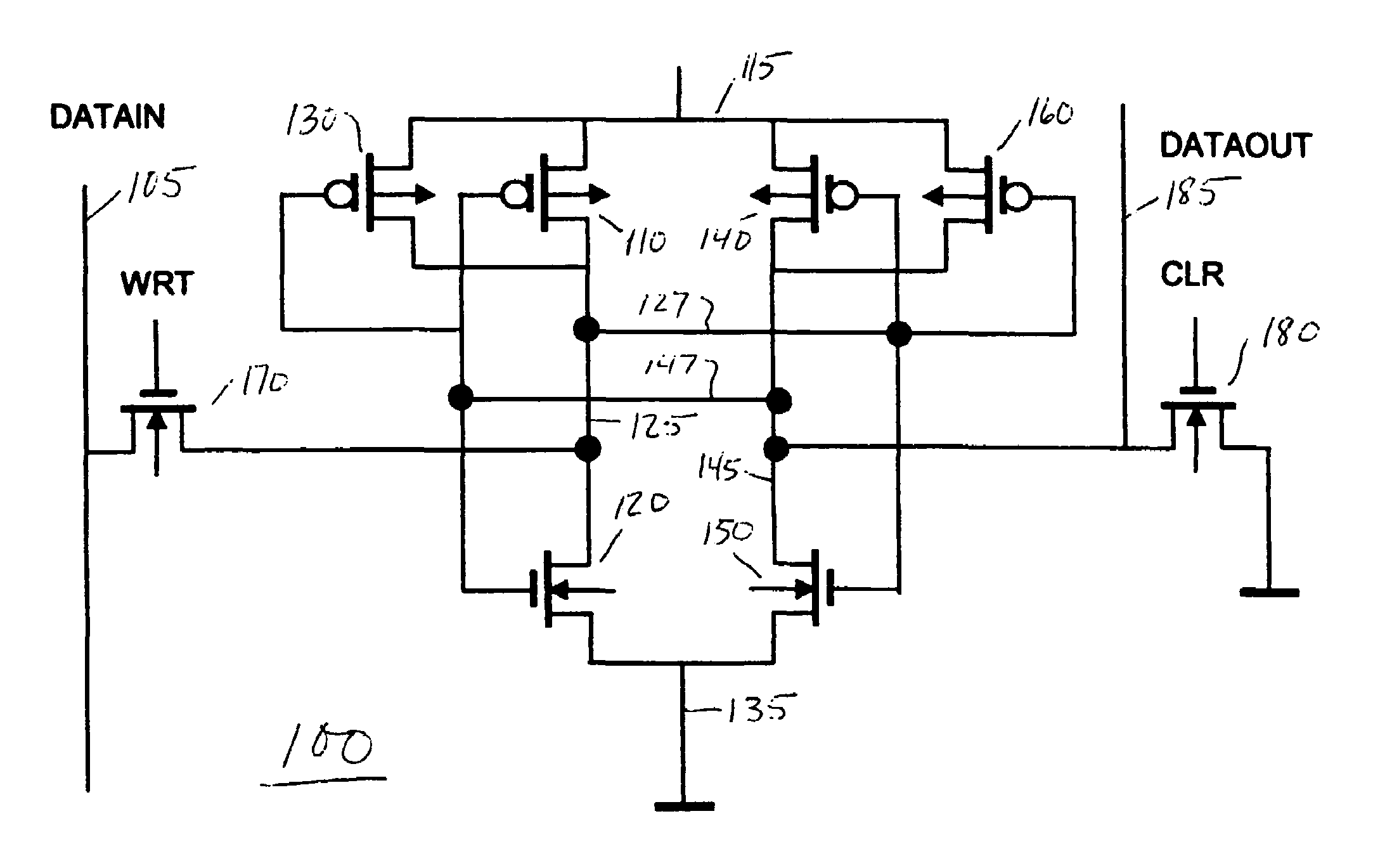
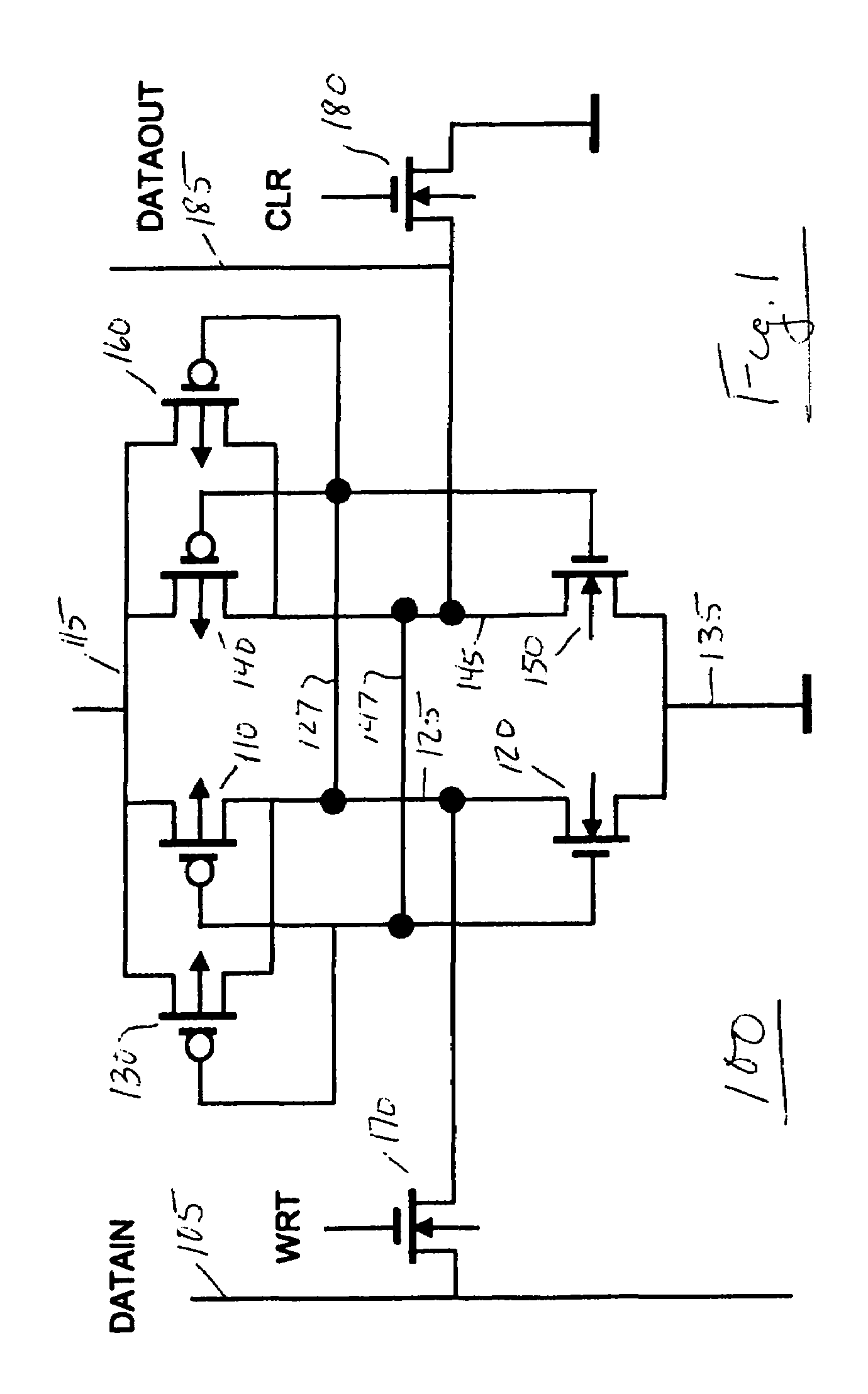
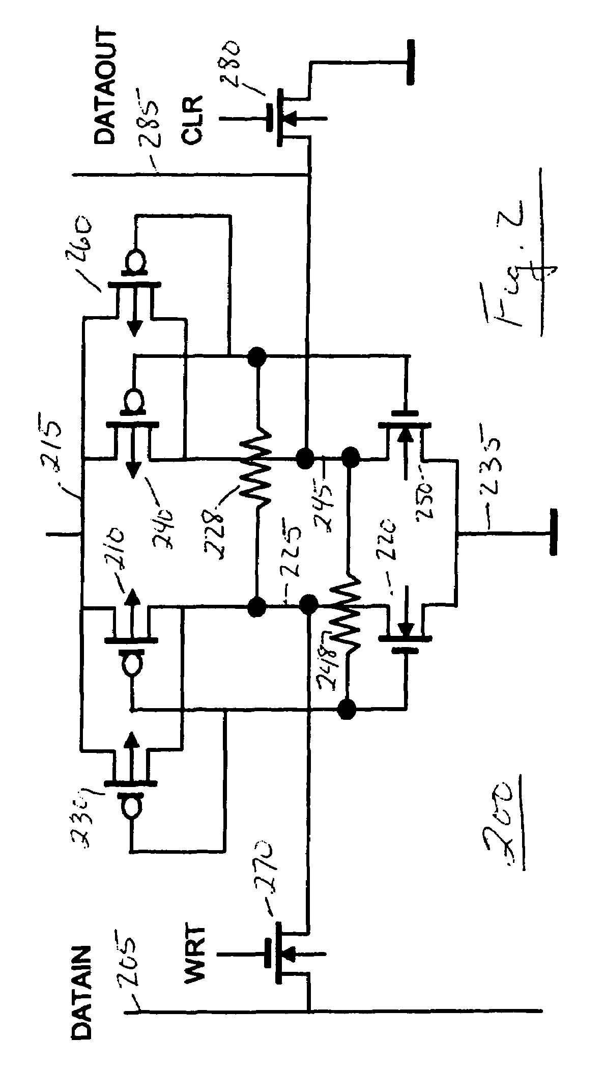
[0016]FIG. 3 depicts an illustrative embodiment of a latch circuit 300 of the present invention comprising eight MOS transistors 310, 320, 330, 340, 350, 360, 370 and 380. Each MOS transistor has a source, a drain and a gate. Transistors 310, 330, 340 and 360 are preferably PMOS transistors; and transistors 320, 350, 370 and 380 are preferably NMOS transistors. The first and second transistors 310, 320 are connected in series such that a source and drain of the first transistor 310 are connected between a first node 315 and a second node 325 and the source and drain of the second transistor are connected between a third node 335 and the second node 325. The fourth and fifth transistors 340, 350 are connected in series such that a source and drain of the fourth transistor 340 are connected between the first node 315 and a fourth node 345 and the source and drain of the fifth transistor 350 are connected between the third node 335 and the fourth node 345. The first node is connected t...


PUM


Abstract

A latch circuit comprises eight MOS transistors in which a first pair of transistors are connected in series between a voltage supply node and ground and a second pair of transistors are connected in parallel to the first pair between the voltage supply node and ground. A fifth transistor is connected between the gates of the first pair and a node between the transistors of the second pair and a sixth transistor is connected between the gates of the second pair and a node between the transistors of the first pair. The seventh transistor is a write transistor connected between a data in line and the node between the first pair of transistors and the eighth transistor is a clear transistor connected between the node between the second pair of transistors and ground.

Description

FIELD OF THE INVENTION[0001]This relates to a latch circuit and a method of operating it.BACKGROUND OF THE INVENTION[0002]FIG. 1 depicts a prior art latch circuit 100 comprising eight MOS transistors 110, 120, 130, 140, 150, 160, 170 and 180. Each MOS transistor has a source, a drain and a gate. Transistors 110, 130, 140, and 160 are preferably PMOS transistors; and transistors 120, 150, 170 and 180 are preferably NMOS transistors. The first and second transistors 110, 120 are connected in series such that a source and drain of the first transistor 110 are connected between a first node 115 and a second node 125 and the source and drain of the second transistor are connected between a third node 135 and the second node 125. The third transistor 130 is connected in parallel with the first transistor 110 so that its source and drain are also connected between the first node and the second node. The fourth and fifth transistors 140, 150 are connected in series such that a source and dr...

Claims


Application Information

Patent Timeline
IPC IPC(8): G11C11/00
CPCG11C11/4125
Inventor XU, YANZHONGWATT, JEFFREY T.
Owner ALTERA CORP
Why Eureka
Eureka Blog
Learn More