Processing of signals from image sensing apparatus whose image sensing area includes a plurality of areas

Inactive Publication Date: 2008-09-09
CANON KK
View PDF32 Cites 23 Cited by
  • Summary
  • Abstract
  • Description
  • Claims
  • Application Information

AI Technical Summary

Benefits of technology

[0014]According to the present invention, an image processing apparatus comprises: an image sensor formed from a plurality of areas each including a plurality of pixels; and a corrector adapted to correct signals output from the plurality of

Problems solved by technology

Forming a sensor with this length from one sensor chip is less advantageous in terms of the technique and cost.
The density is different between adjacent chips, seriously degrading the quality.
The levels of read signals differ from each other at the halftone level, resulting in a density difference and

Method used


Image

  • Processing of signals from image sensing apparatus whose image sensing area includes a plurality of areas
  • Processing of signals from image sensing apparatus whose image sensing area includes a plurality of areas
  • Processing of signals from image sensing apparatus whose image sensing area includes a plurality of areas

Examples


first embodiment

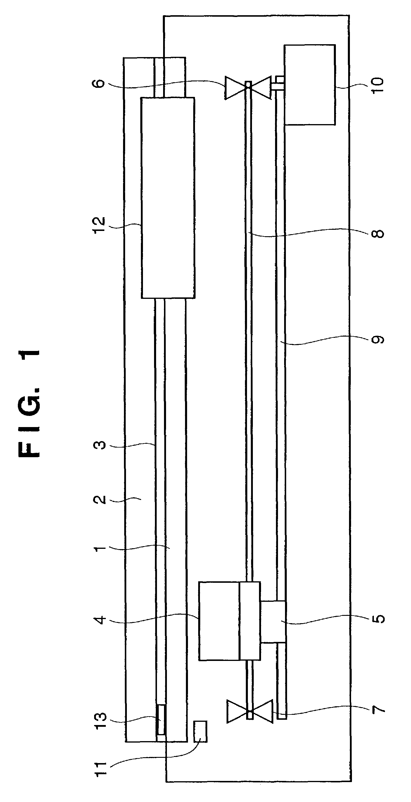
[0050]The arrangement of the image reader of an image processing apparatus according to the first embodiment will be described with reference to FIG. 1.

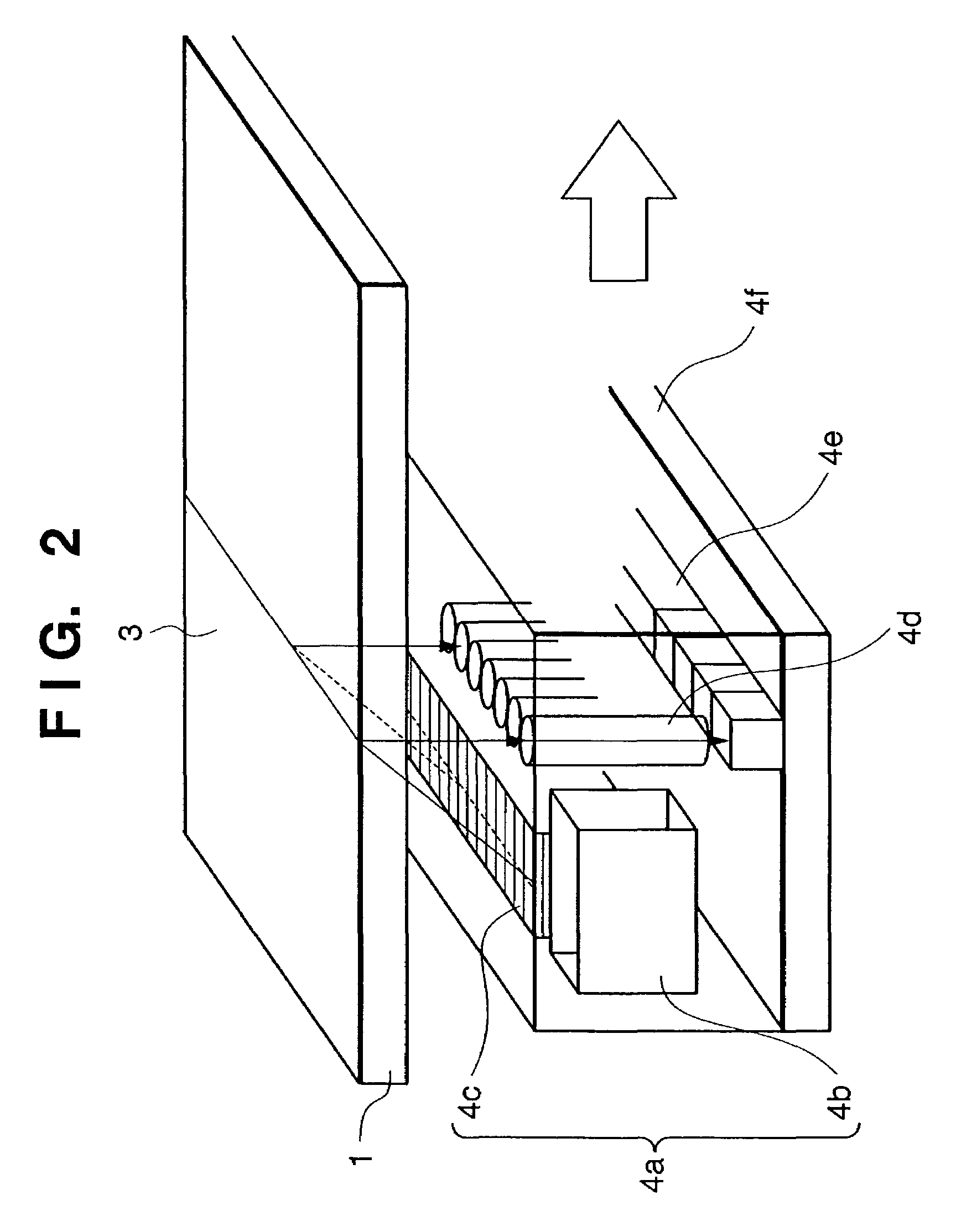
[0051]Reference numeral 1 denotes a platen glass on which a document is set; 2, a platen cover which presses the platen glass and can be opened / closed; 3, a document set on the platen glass; 4, a contact image sensor (to be referred to as a “CIS” hereinafter) serving as a scanning optical system for reading the image of the document 3; 5, a carriage which holds the CIS; 9, a shaft serving as a guide when the carriage is moved in the sub-scanning direction in reading a document; 8, a timing belt fixed to the carriage 5; 6 and 7, pulleys which are arranged at the two ends of the timing belt so as to smoothly move the timing belt 8; 10, a stepping motor which is connected to either the pulley 6 or 7 and drives the pulley 6 or 7; 11, a home position sensor for detecting the sub-scanning position of the carriage 5 held by the CIS 4; 13, a...

second embodiment

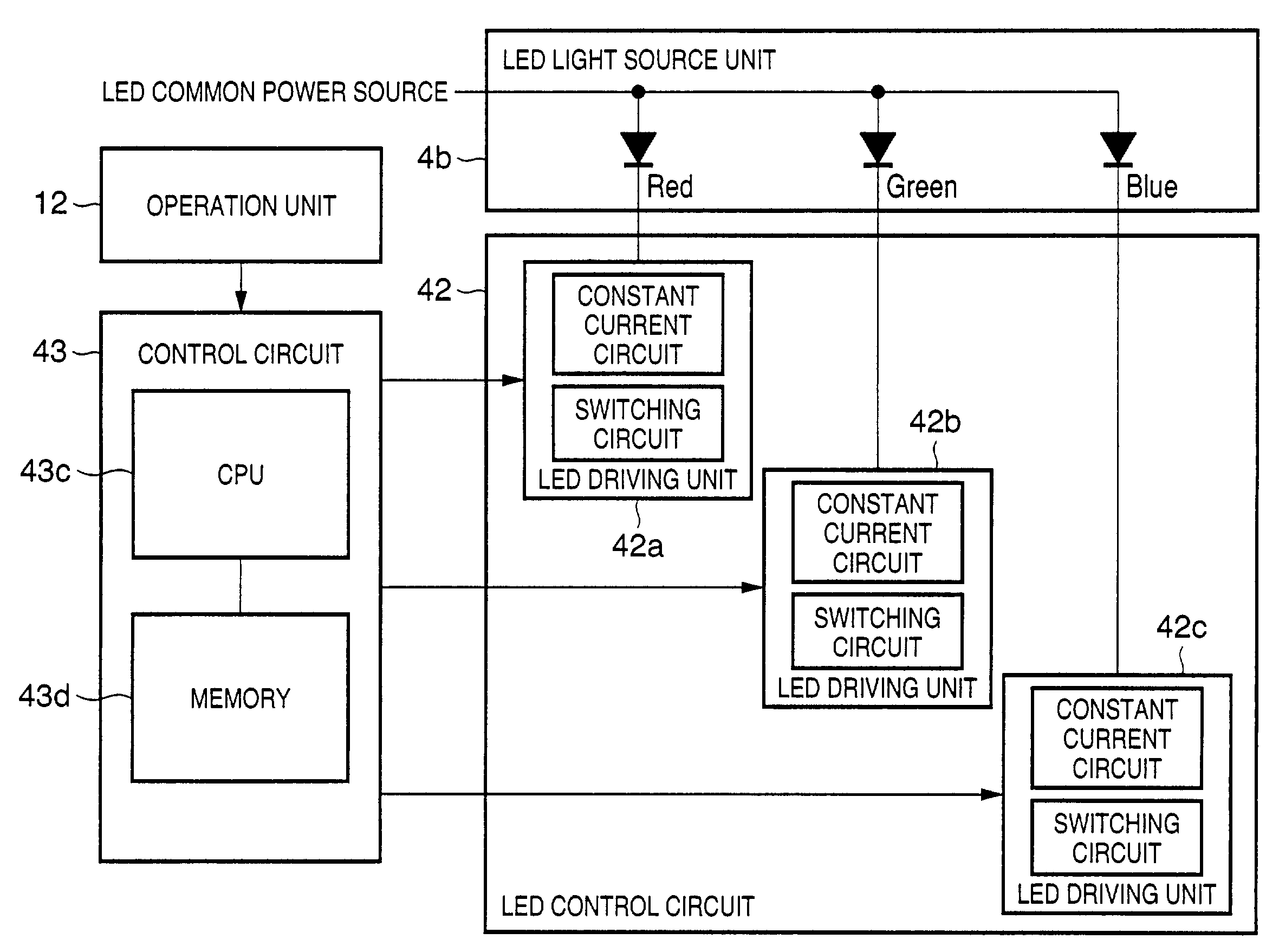
[0119]FIG. 10 is a block diagram showing an image processing apparatus according to the second embodiment of the present invention.

[0120]Reference numeral 202 denotes a contact image sensor (CIS) module having a multi-chip sensor functioning as an image sensing unit which includes a plurality of pixels and a plurality of output units for outputting signals from the pixels. In a multi-chip sensor 2024, as shown in FIG. 11, a plurality of sensor chips (chip1 to chip16 in FIG. 11) on each of which a plurality of pixels are arrayed in one direction (main scanning direction) are arrayed on a mounting substrate 2025 in the same direction as that of the pixel array.

[0121]The arrangement of the CIS module 202 in the second embodiment will be described.

[0122]In the CIS module 202, as shown in FIG. 12, a cover glass 2021, an illumination light source 2022 formed from an LED, a ×1 imaging lens 2023, such as a SELFOC lens, and the multi-chip sensor 2024 are mounted on the substrate 2025. These ...

third embodiment

[0189]The third embodiment will be explained. Only the difference from the second embodiment will be described, and a description of the same part will be omitted.

[0190]FIG. 21 is a block diagram showing an image processing apparatus according to the third embodiment of the present invention.

[0191]Reference numeral 213 denotes a center-division two-end-read type CCD image sensor serving as an image sensing unit which includes a plurality of pixels and a plurality of output units for outputting signals from the pixels.

[0192]FIG. 22 is a block diagram for explaining details of the CCD image sensor 213.

[0193]Reference symbols P1, P2, . . . , P7500 denote photodiodes as photoelectric converters which read and accumulate image information for 7,500 pixels in the main scanning direction. The sensor is divided into left and right parts at the boundary between the 3750th and 3751st central pixels. Charges in the photodiodes are transferred to CCD analog shift registers 2131, 2133, 2135, and...


PUM


Abstract

An image processing apparatus includes an image sensor formed from a plurality of areas each including a plurality of pixels, and a corrector adapted to correct signals from the plurality of areas of the image sensor. The corrector has a plurality of correction data smaller in number than the areas, and performs correction by selectively using the correction data for each area of the image sensor.

Description

FIELD OF THE INVENTION[0001]The present invention relates to an image processing apparatus having an image sensing apparatus and a correction method and, more particularly, to an image processing apparatus in which an image sensing apparatus has a plurality of areas each including a plurality of pixels and processes signals output from the plurality of areas, and a correction method.BACKGROUND OF THE INVENTION[0002]Contact image sensors (CISs) have recently been developed and put into practical use along with reductions in size and weight in a scanner apparatus for inputting an image to a personal computer and the document reader of a facsimile apparatus. The contact image sensor is formed from a light source, rod lenses which implement a ×1 erect optical system, and a one-dimensional light-receiving sensor whose effective width is substantially the same as the maximum width of a document to be read. The CIS can shorten the optical path length of an optical system, compared to an op...

Claims


Application Information

Patent Timeline
IPC IPC(8): H04N1/40H04N1/401
CPCH04N1/401
Inventor TANABE, MASATOSHIHIROMATSU, KENJISUGETA, MITSUHIRO
Owner CANON KK
Why Eureka
Try Eureka