Symmetric bipolar junction transistor design for deep sub-micron fabrication processes

a technology of bipolar junction transistors and fabrication processes, applied in the direction of transistors, semiconductor devices, electrical equipment, etc., can solve the problems of new design constraints affecting the operating characteristics of certain devices

Inactive Publication Date: 2008-10-21
INTEL CORP
View PDF5 Cites 64 Cited by
  • Summary
  • Abstract
  • Description
  • Claims
  • Application Information

AI Technical Summary

Problems solved by technology

As the drive to produce smaller devices in integrated circuit design continues, the result of producing smaller devices brings about new design constraints that affect the operating characteristics of certain devices.

Method used


Image

  • Symmetric bipolar junction transistor design for deep sub-micron fabrication processes
  • Symmetric bipolar junction transistor design for deep sub-micron fabrication processes
  • Symmetric bipolar junction transistor design for deep sub-micron fabrication processes

Examples


Embodiment Construction

[0013]In the following description numerous specific details are set forth in order to provide an understanding of the claims. One of ordinary skill in the art will appreciate that these specific details are not necessary in order to practice the disclosure. In other instances, well-known semiconductor fabrication processes and techniques have not been set forth in particular detail in order to not unnecessarily obscure embodiments of the present invention.

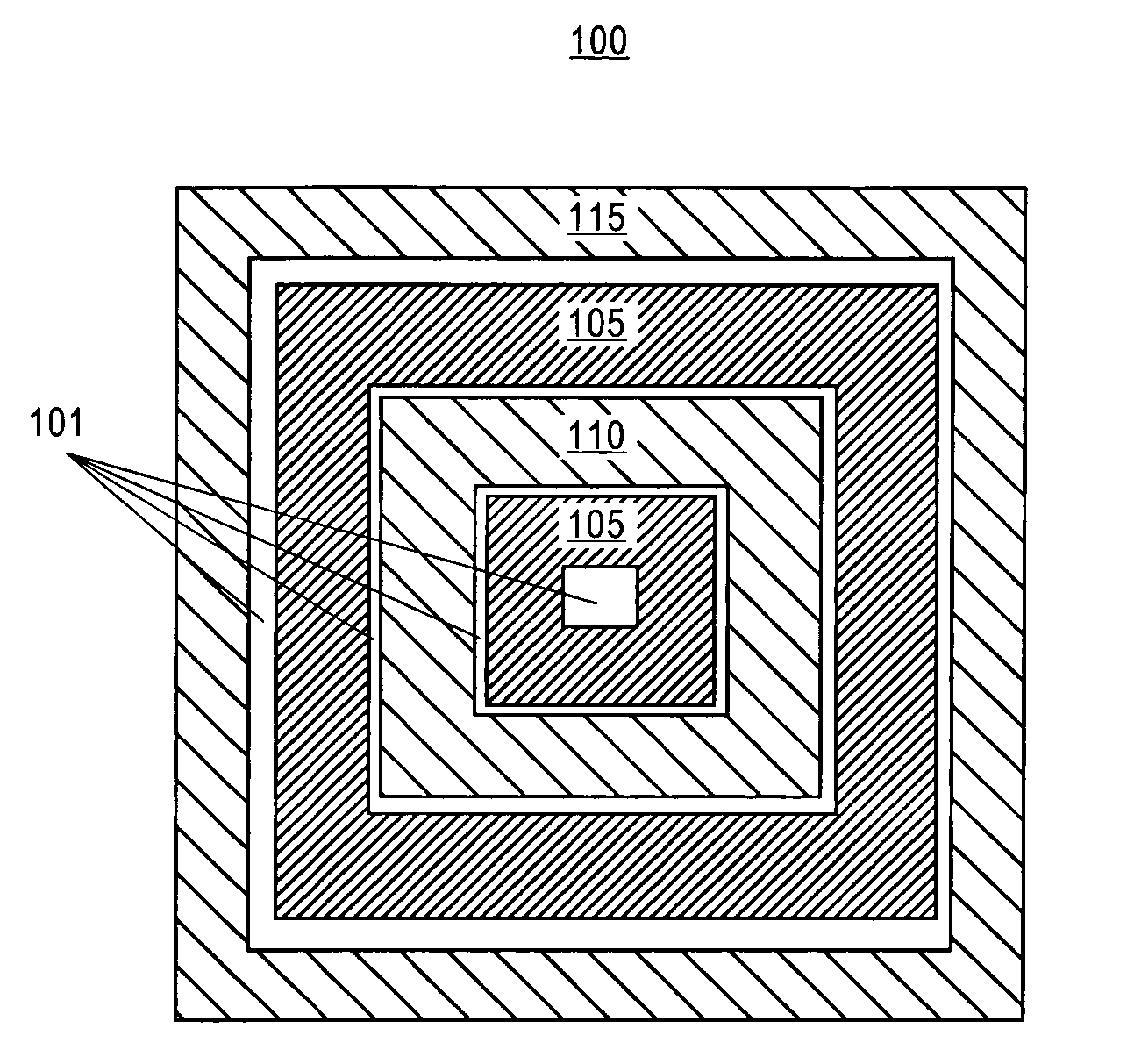
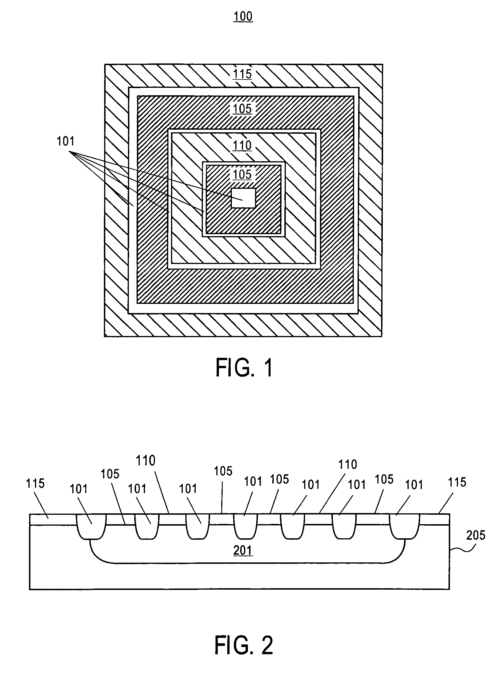
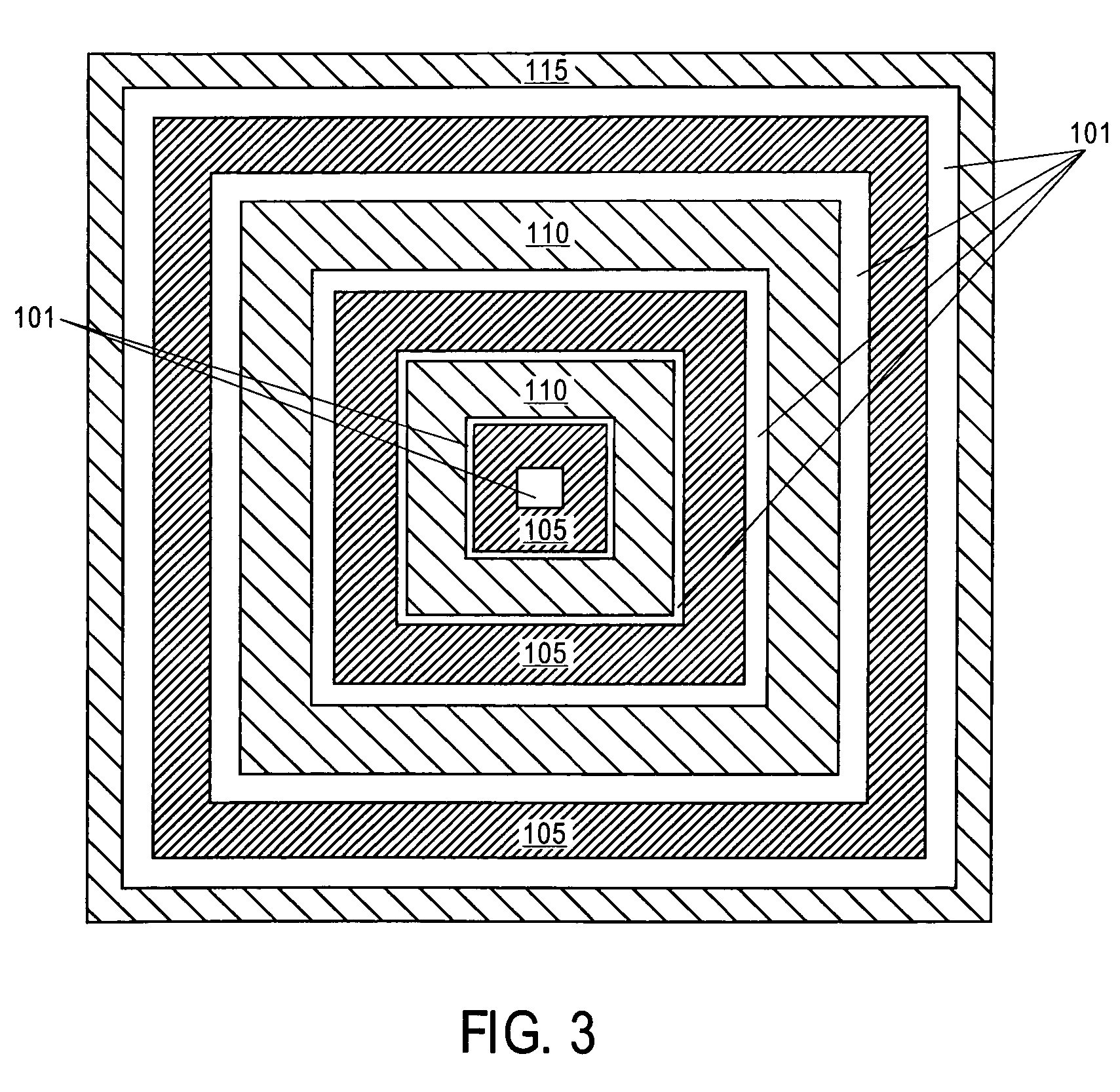
[0014]Embodiments of the present invention include a design of a bipolar junction transistor (BJT) and a manufacturing process thereof that preserves symmetry of a bipolar junction transistor while conforming to design constraints including a restriction on a maximum dimension of a diffusion region in either the X or Y direction. The design uses a ring geometry to preserve symmetry of a bipolar junction transistor while adhering to design constraints of a semiconductor fabrication process such as a maximum diffusion width dimensio...


PUM


Abstract

Described herein are embodiments of a bipolar junction transistor including a plurality of base terminal rings having an emitter terminal ring between any two base terminal rings of the plurality of base terminal rings, and a collector terminal ring surrounding the plurality of base terminal rings and the emitter terminal ring and methods of manufacturing the same.

Description

BACKGROUND OF THE INVENTION[0001]1. Field of the Invention[0002]the present invention relates to the field of semiconductor devices and more specifically to a bipolar junction transistor structure and its method of fabrication.[0003]2. Discussion of Related Art[0004]In bipolar junction transistor (BJT) design the need for device symmetry is necessary to ensure optimum device performance and optimal matching between devices. Proper matching between connected devices, allows the use of averaging techniques to cancel out linear and non-linear gradients induced by manufacturing processes. Averaging can be applied to the bipolar junction transistor by arranging stripes or rectangles of alternating diffusion types that constitute the bipolar junction transistor. Further improvements can be achieved with symmetry. Such averaging techniques allow a bipolar junction transistor to be used in high precision circuits such as bandgap voltage references, thermal sensors, and on-die thermal calibr...

Claims


Application Information

Patent Timeline
Patent Type & Authority Patents(United States)
IPC IPC(8): H01L27/082
CPCH01L29/0692H01L29/0804H01L29/66272H01L29/7322H01L29/73H01L21/8222
Inventor ARENDT, KEVIN E.
Owner INTEL CORP
Why Eureka
Try Eureka