High power shunt switch with high isolation and ease of assembly

a high-efficiency, shunt switch technology, applied in the direction of electrical equipment, semiconductor devices, semiconductor/solid-state device details, etc., can solve the problems of significant disadvantages of cob-mounted diodes, already and even more expensive cob assembly process

Active Publication Date: 2008-10-21
MACOM TECH SOLUTIONS HLDG INC
View PDF14 Cites 46 Cited by
  • Summary
  • Abstract
  • Description
  • Claims
  • Application Information

AI Technical Summary

Problems solved by technology

There are, however, significant disadvantages associated with COB-mounted diodes.
For example, since wire bonds are exposed during most of the COB assembly process, the wire bonds routinely become damaged, making the already expensive COB assembly process even costlier.
Additionally, since the number of components that may be mounted near COB-mounted diodes is limited, relatively large PCBs are required.
Packaged diodes, however, also have their own set of drawbacks.
One of the most recognized drawbacks of packaged diodes is the existence of ‘package parasitics’.
Package parasitics are unwanted electrical and mechanical attributes that result from the physical construction of the package itself.
This inductance limits the isolation of the packaged diode 100, particularly at high frequencies, which results in reduced overall performance.

Method used


Image

  • High power shunt switch with high isolation and ease of assembly
  • High power shunt switch with high isolation and ease of assembly
  • High power shunt switch with high isolation and ease of assembly

Examples


Embodiment Construction

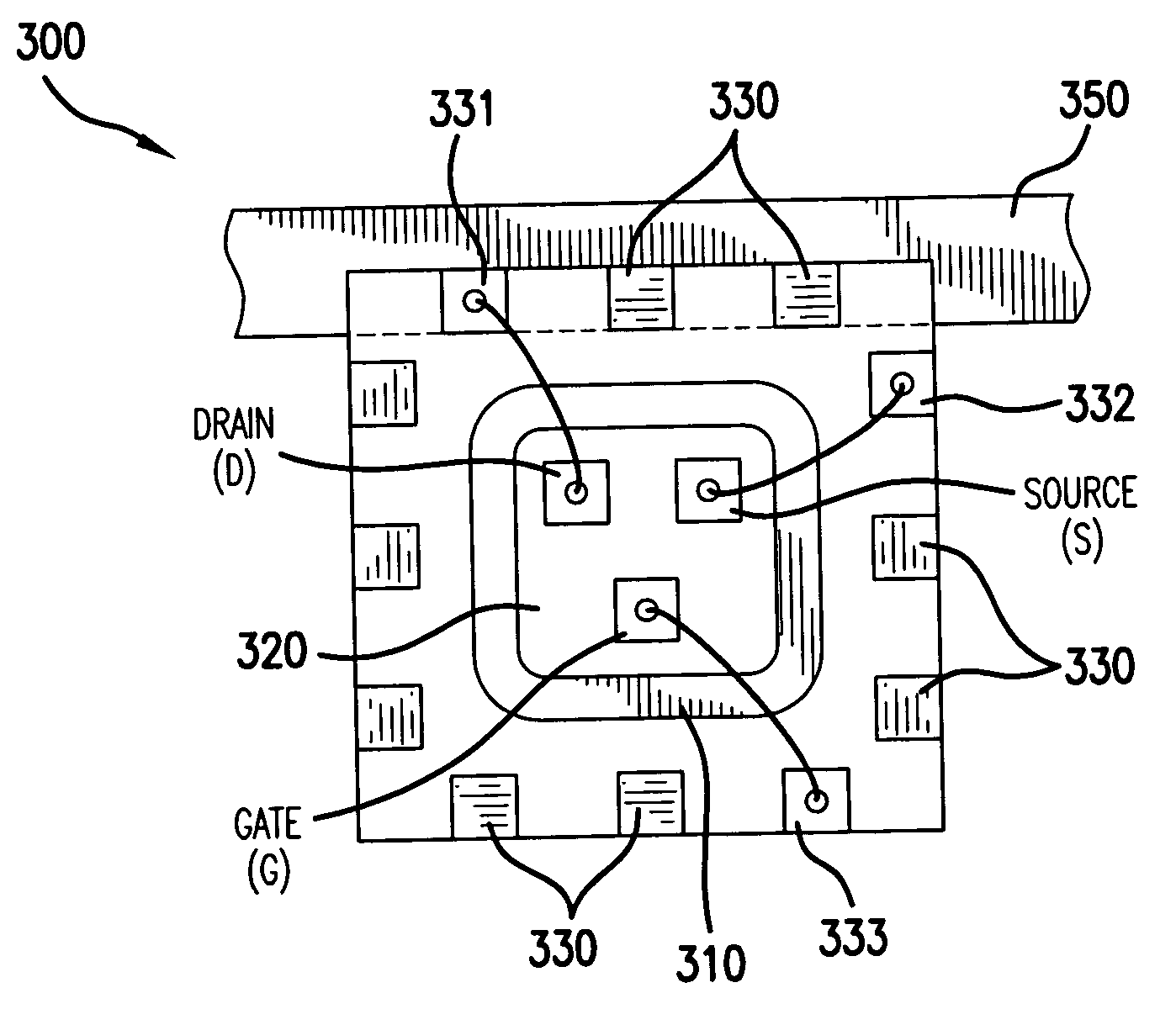
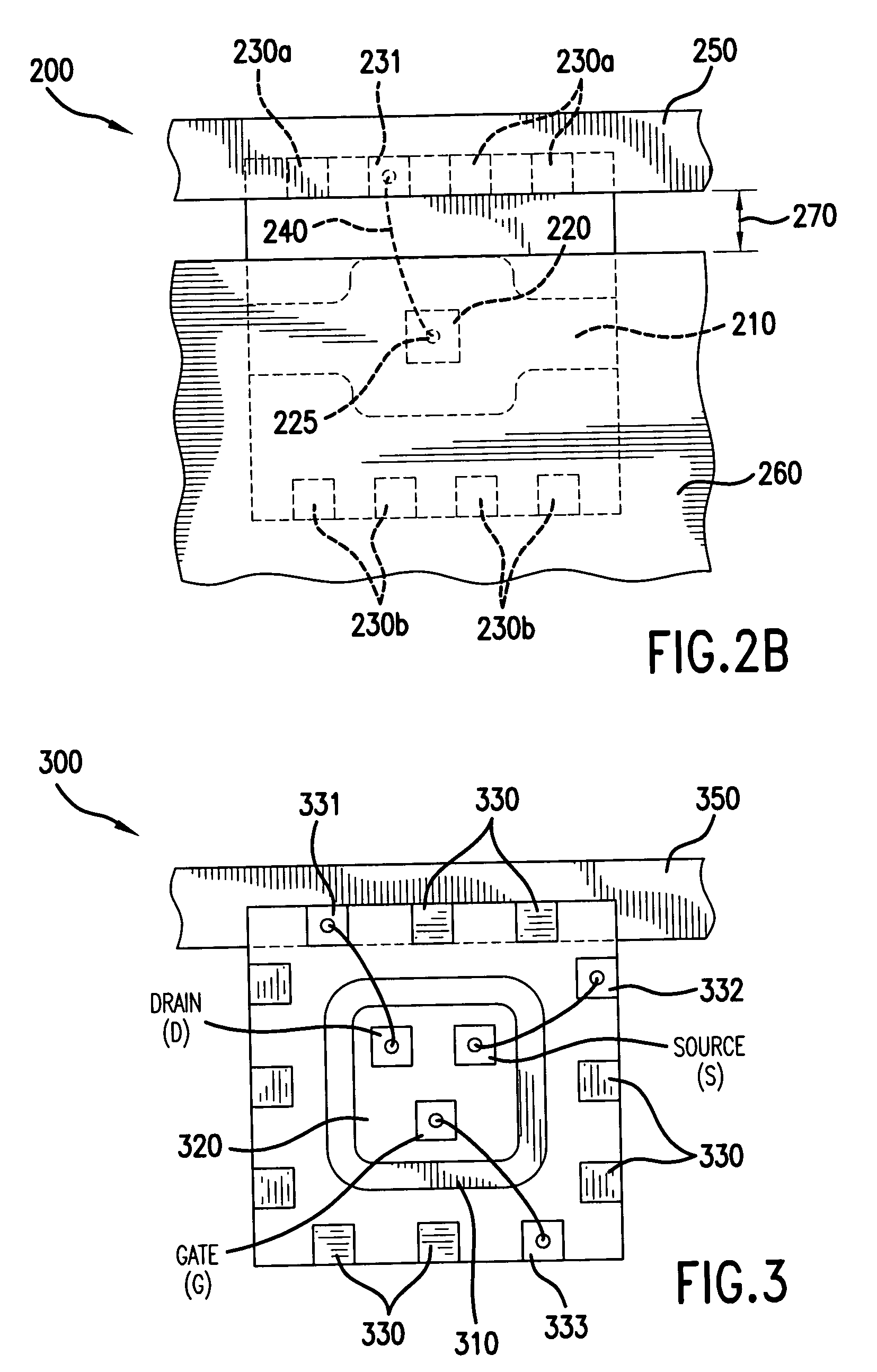
[0017]Described herein is a novel lead-less package structure for use in high power shunt switch applications. Unlike existing packages, the package structure of the present invention offers high isolation, ease of assembly, and low package parasitics. In addition, the present invention provides a flexible design that may be modified according to the particular implementation for improved power handling and isolation.

[0018]In a preferred embodiment, the package structure of the present invention comprises a leadframe that includes a paddle and a plurality of bond pads, a shunt element, a wire bond and an encapsulant. The leadframe is positioned such that the paddle is located along a center portion of the package. Preferably, the paddle is configured to extend from one end of the package to another end. The plurality of bond pads are preferably located about a periphery of the leadframe, with one-half of the bond pads positioned in a substantially straight line on either side of the...


PUM


Abstract

A high power shunt switch comprises a leadframe including a paddle for supporting a shunt element, and a plurality of bond pads located around a periphery of the paddle, wherein at least a first subset of the bond pads are aligned in a substantially straight-line configuration. A shunt element is fixedly attached to the paddle and wire bonded to a top surface of one the bond pads. An encapsulant is disposed on the paddle, the shunt element, the plurality of bond pads, and the wire bond, thereby forming an encapsulated package structure. The package structure is positioned and attached to a transmission line such that the bottom surfaces of each of the at least first subset of bond pads are in simultaneous contact with the transmission line. The package structure and the transmission line are fixedly attached to a suitable substrate.

Description

FIELD OF INVENTION[0001]The present invention relates generally to a high power shunt switches. More particularly, the present invention relates to a method and apparatus for providing a package structure for use in high power shunt switch applications.BACKGROUND[0002]High-power switches are typically fabricated using shunt-connected diodes. As known to those skilled in the art, shunt-connected diodes are preferred in high power switch applications because they provide high-isolation when in an ON state, minimize losses when in an OFF state, and because of their cost effectiveness as compared to mechanical switches.[0003]In conventional applications, diodes may be mounted to substrates, such as printed circuit boards (PCBs), using a chip-on-board (COB) mounting scheme. Chip-On-Board is essentially the attachment of a die, in this case a diode, directly onto the surface of a PCB. Electrical contacts of the diode are wire bonded to conductors on the PCB. An encapsulant is then dispose...

Claims


Application Information

Patent Timeline
Patent Type & Authority Patents(United States)
IPC IPC(8): H01L23/495
CPCH01L23/49575H01L23/66H01L23/49562H01L2223/6627H01L2224/48091H01L2224/48247H01L2924/19033H01L2924/30107H01L2924/3011H01L2924/00014H01L24/48H01L2924/13063H01L2924/00H01L2224/45099H01L2224/45015H01L2924/207
Inventor WEIGAND, CHRISTOPHER D.
Owner MACOM TECH SOLUTIONS HLDG INC
Why Eureka
Try Eureka