High power LED package with universal bonding pads and interconnect arrangement
a technology of led chips and interconnections, applied in the field of high-power led packages, can solve the problems of limited use of led chips, prior art packages providing inadequate heat dissipation away from led dies, and current led packages cannot handle the high-power density of led chips
- Summary
- Abstract
- Description
- Claims
- Application Information
AI Technical Summary
Problems solved by technology
Method used
Image
Examples
Embodiment Construction
1. An Overview
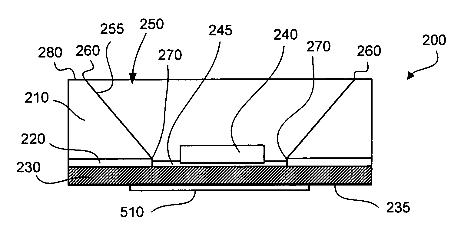
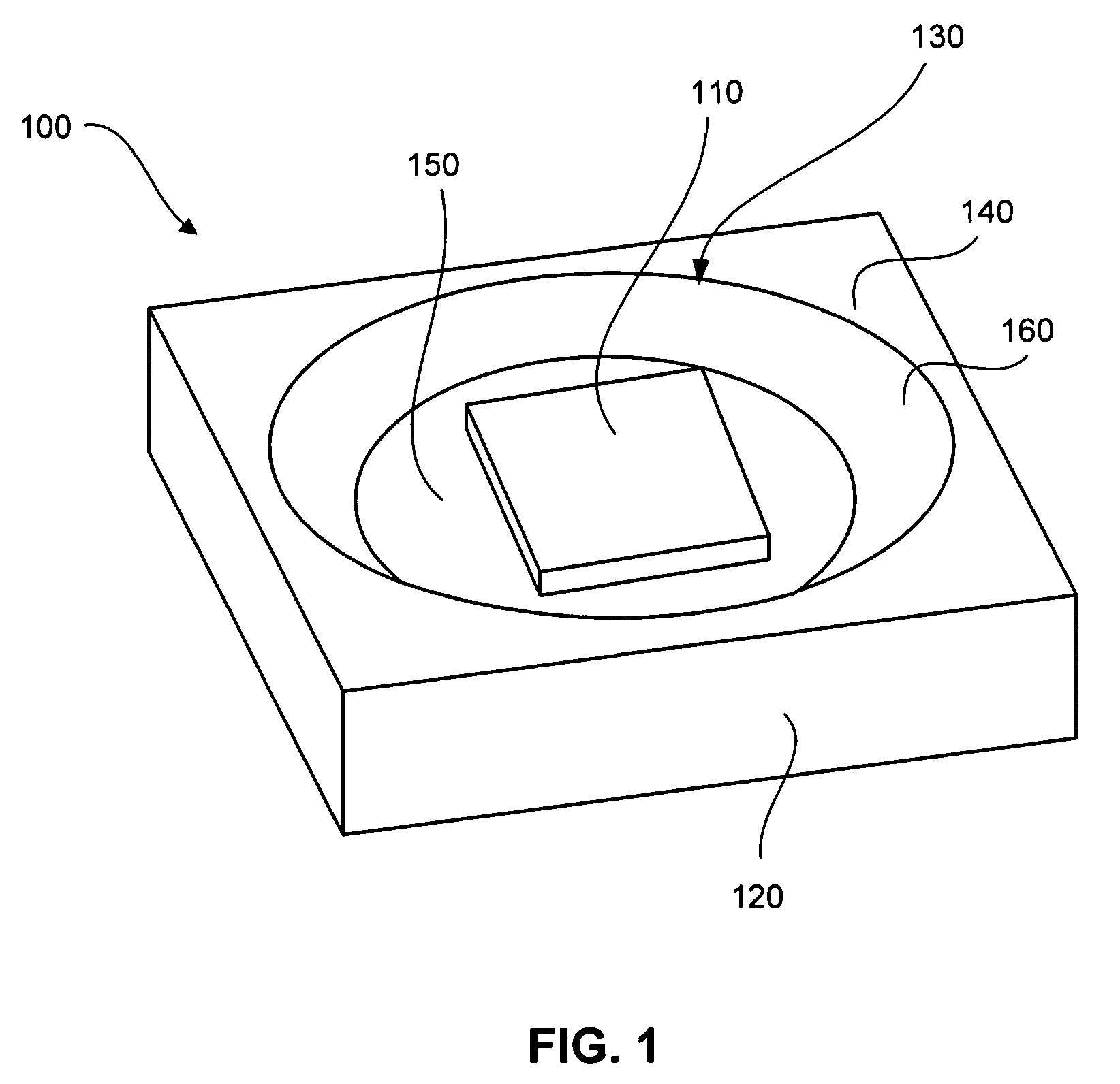
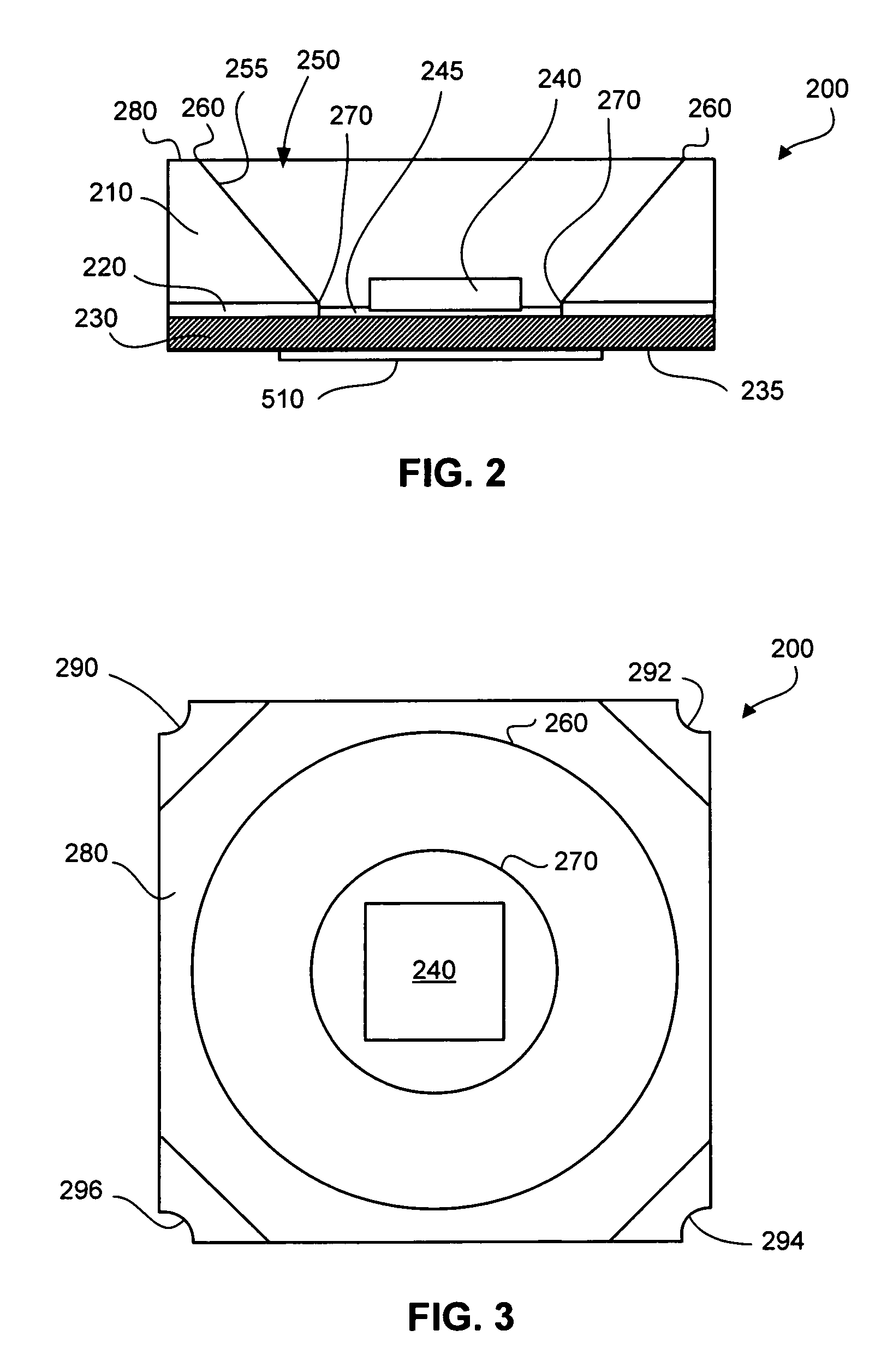
[0029]The present disclosure provides LED packages with structures and materials that provide higher heat dissipation than presently available. A further benefit of the present invention is improved matching of the coefficients of thermal expansion (CTEs) of the LED dies and the materials to which they are bonded for higher reliability. Due to the improved heat conduction, the packages of the present invention allow high-power LEDs to operate at full capacity. Improved heat conduction also allows for both smaller packages and devices within which packages are placed more closely together.
[0030]One measure of how efficiently a package dissipates heat is the temperature rise across the package. Using this measure, in current high-power LED packages the thermal resistance from the junction to the case is generally in the range of 15 to 20° C. / W. By comparison, an exemplary embodiment of the present disclosure has a lower thermal resistance of only about 6° C. / W or 3° C. / W...
PUM
 Abstract
Description
Claims
Application Information


