
Liquid crystal display

a liquid crystal display and display technology, applied in static indicating devices, instruments, non-linear optics, etc., can solve the problems of reduced resistance of common lines, easy distortion of common voltage, and luminance difference between upper and lower, so as to reduce the distortion of common voltage and optimally dispose of common lines

Active Publication Date: 2010-05-06
LG DISPLAY CO LTD
View PDF6 Cites 35 Cited by
  • Summary
  • Abstract
  • Description
  • Claims
  • Application Information

AI Technical Summary

Benefits of technology

[0010]Embodiments of the invention provide a liquid crystal display capable of reducing a distortion of a common voltage by optimally disposing common lines.
[0011]Embodiments of the invention also provide a liquid crystal display capable of increasing an aperture ratio of a pixel array by optimally disposing common lines.

Problems solved by technology

However, the common voltage is easily distorted by a resistance of the common line or a deviation of the common voltage over the entire surface of a liquid crystal display panel depending on a structure of the common line.
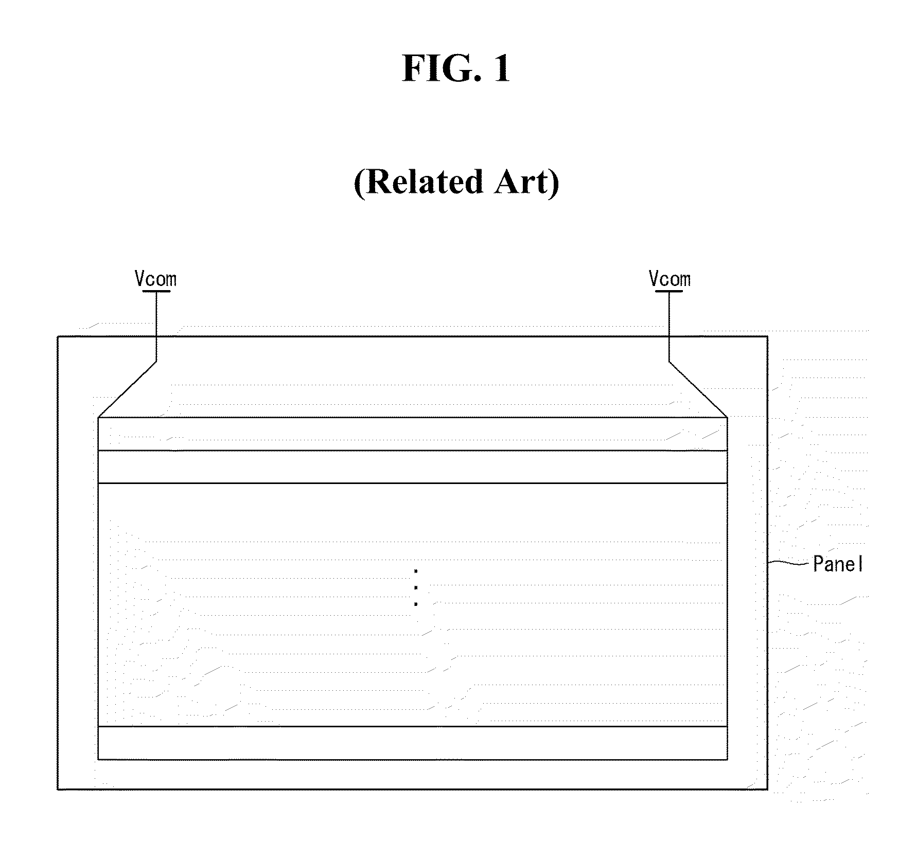
However, as shown in FIG. 1, because a related art liquid crystal display has a structure to receive a common voltage Vcom through only two input units, it is limited to a reduction in resistances of common lines.
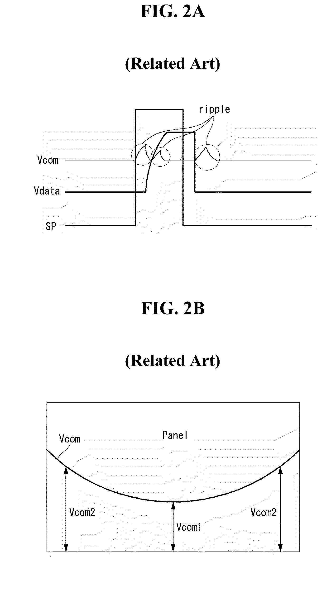
The deviation of the common voltage Vcom, as shown in FIG. 3B, causes a luminance difference between upper and lower portions of the liquid crystal display panel and a flicker, and also accumulates a DC component inside the panel to cause image sticking.
However, it is limited to a reduction in the resistances of the common lines because of the limited size of the non-display area.
Further, there is a relatively large deviation among resistances of the common lines depending on locations of the common lines.
Further, because as many common lines as the number of horizontal lines are needed in the related art liquid crystal display, it is limited to an increase in a luminance by increasing an aperture ratio of a pixel array.

Method used


Image

  • Liquid crystal display
  • Liquid crystal display
  • Liquid crystal display

Examples


Embodiment Construction

[0056]Reference will now be made in detail embodiments of the invention examples of which are illustrated in the accompanying drawings.

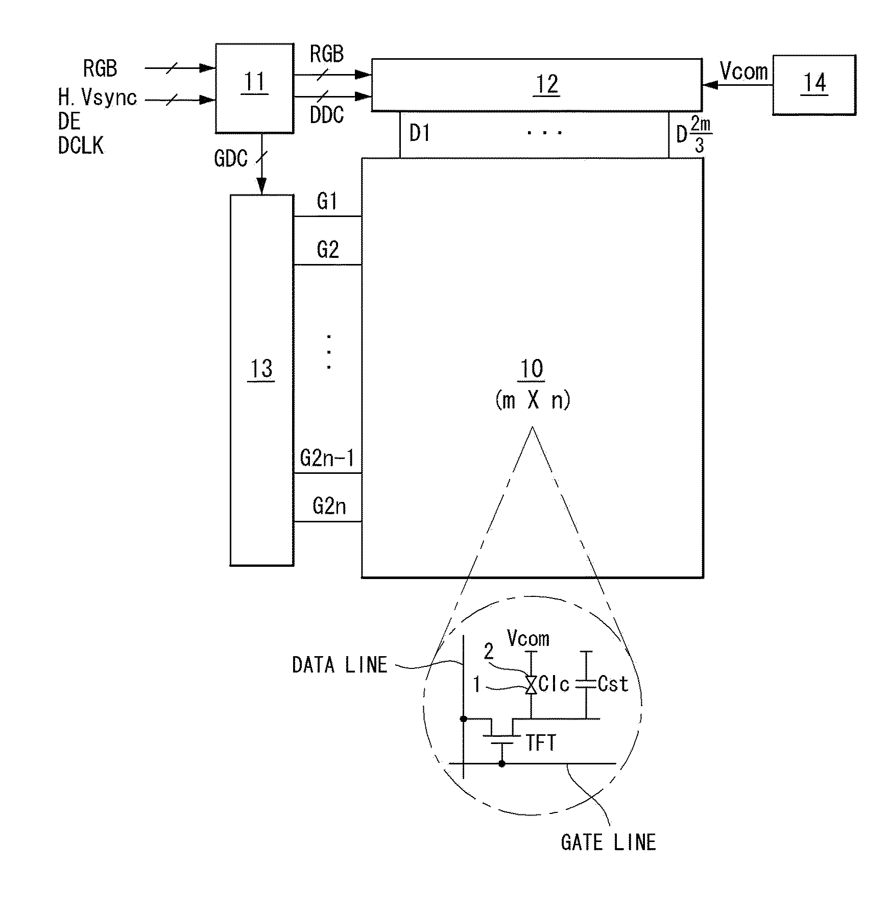
[0057]FIG. 4 is a block diagram showing an exemplary configuration of a liquid crystal display according to an embodiment of the invention.

[0058]As shown in FIG. 4, a liquid crystal display according to an embodiment of the invention includes a liquid crystal display panel 10, a timing controller 11, a data drive circuit 12, a gate drive circuit 13, and a common voltage generation unit 14.

[0059]The liquid crystal display panel 10 includes an upper glass substrate, a lower glass substrate, and a liquid crystal layer between the upper and lower glass substrates. The liquid crystal display panel 10 includes m×n liquid crystal cells Clc (i.e., m×n subpixels) (m and n are positive integer) arranged in a matrix format at each crossing of 2m / 3 data lines D1 to D(2m / 3) and 2n gate lines G1 to G2n. Two gate lines and two data lines are assigned to each pixel ...


PUM


Abstract

A liquid crystal display is provided. In the liquid crystal display, a common line includes an edge common line that is formed in a non-display area outside a display area of a liquid crystal display panel to receive a common voltage through a plurality of input units, a plurality of pixel common line patterns that are formed along edges of each of subpixels to be electrically connected to one another, and a plurality of longitudinal common lines that is electrically connected to the edge common line to apply the common voltage to the pixel common line patterns. Each of the pixel common line patterns has a mesh structure and is connected to common electrodes of the subpixels. Each of the longitudinal common lines is formed between two horizontally adjacent pixels in a direction parallel to the data lines.

Description

[0001]This application claims the benefit of Korea Patent No. 10-2008-0107355 filed on Oct. 30, 2008, the entire contents of which is incorporated Application herein by reference for all purposes as if fully set forth herein.BACKGROUND OF THE INVENTION[0002]1. Field of the Invention[0003]Embodiments of the invention relate to a liquid crystal display capable of reducing a distortion of a common voltage.[0004]2. Discussion of the Related Art[0005]Active matrix type liquid crystal displays display a moving picture using a thin film transistor (TFT) as a switching element. The active matrix type liquid crystal displays have been implemented in televisions as well as display devices in portable devices, such as office equipment and computers, because of the thin profile of an active matrix type liquid crystal displays. Accordingly, cathode ray tubes (CRT) are being rapidly replaced by active matrix type liquid crystal displays.[0006]In the active matrix type liquid crystal displays, a d...

Claims


Application Information

Patent Timeline
IPC IPC(8): G02F1/1345
CPCG02F1/134363G02F1/1345G02F1/136286G02F2201/121G09G3/3614G09G2300/0426G09G2300/0439G02F1/1343G02F1/133
Inventor LEE, JAEKYUNOH, JAEYOUNGSHIN, DONGSUCHOI, DAEJUNGCHOI, SANGHUN
Owner LG DISPLAY CO LTD
Learn More