Sub-assembly

a technology of sub-assembly and semiconductor module, which is applied in the direction of semiconductor device details, cooling/ventilation/heating modification, semiconductor/solid-state device details, etc., can solve the problems of mounting errors, complicated and cost-intensive mounting of known power semiconductor module on cooling element,

Active Publication Date: 2009-01-13
INFINEON TECH AG
View PDF5 Cites 11 Cited by
  • Summary
  • Abstract
  • Description
  • Claims
  • Application Information

AI Technical Summary

Problems solved by technology

The mounting of the known power semiconductor module on the cooling element is complicated and cost-intensive because the press-on element / elements has / have to be handled, supplied and mounted separately in the mounting process.
Depending on the configuration of the power semiconductor module and the press-on element, mounting errors may occur in this case—e.g. as a result of defective positioning or orientation—and said mounting errors influence the cooling effect and hence the operational reliability.
Moreover, the connection between power semiconductor module and press-on element involves dimensional tolerances which have an unforeseeable effect on the magnitude of the press-on forces exerted.

Method used


Image

  • Sub-assembly
  • Sub-assembly
  • Sub-assembly

Examples


Embodiment Construction

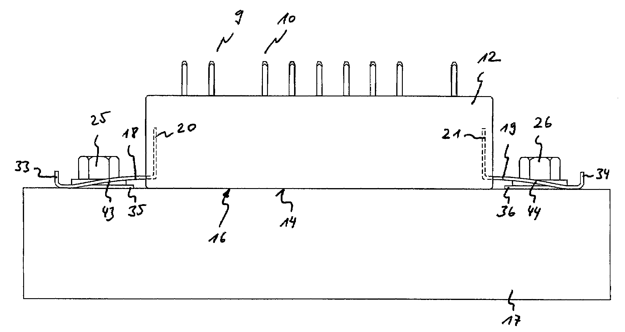
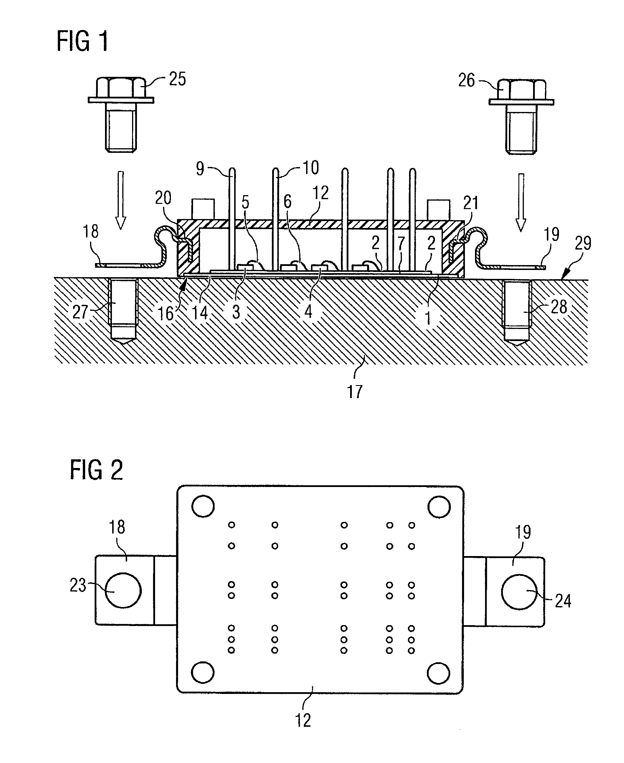
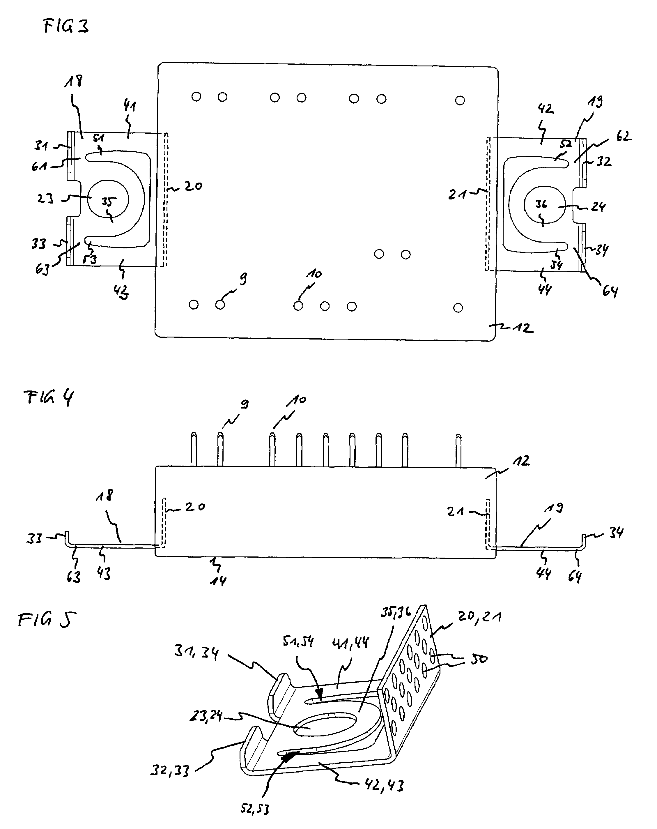
[0014]A power semiconductor module is thermally connected to a cooling element in a simple, cost-effective and reliable manner. According to an embodiment, the power semiconductor module comprises at least one press-on element which is captively connected to the power semiconductor module. The press-on element presses a heat-dissipation contact area of the module onto the cooling element in the mounted state, thereby ensuring a desired reliable thermally conductive contact between the power semiconductor module and cooling element.

[0015]In an embodiment, the press-on element, upon connection of a module to a cooling element, does not have to be separately delivered, stored, handled, supplied and finally mounted at the power semiconductor module. Since the press-on element is configured as an integral element that is captively connected to the power semiconductor module, it advantageously forms an (in this respect prefabricated) sub-assembly for simple and cost-effective mounting on ...


PUM


Abstract

According to an embodiment, a power semiconductor module comprises a heat-dissipation contact area configured to thermally connect the power semiconductor module to a cooling element. The power semiconductor module also comprises a housing and a press-on element. The press-on element comprises an anchoring region and is captively anchored in the housing. A fixing eye is resiliently coupled with the anchoring region.

Description

CROSS-REFERENCE TO RELATED APPLICATION[0001]This application is a continuation-in-part of co-pending U.S. patent application Ser. No. 11 / 682,483 filed Mar. 6, 2007, which is a continuation of International Application No. PCT / EP2005 / 007514 filed Jul. 12, 2005 designating the United States, which claims priority to German application number DE 10 2004 043 019.5 filed Sep. 6, 2004.BACKGROUND OF THE INVENTION[0002]The invention relates to a power semiconductor module comprising a heat-dissipation contact area for thermally conductive connection to a cooling element.[0003]A module construction of this type is customary and known e.g. from DE 199 42 915 A1. Said known module comprises an insulating and thermally conductive carrier (substrate) composed e.g. of a ceramic material coated e.g. with copper (DCB) on both sides. Conductor track structures are formed in the top side coating, a plurality of power semiconductors being electrically connected to the structures. The substrate undersi...

Claims


Application Information

Patent Timeline
Patent Type & Authority Patents(United States)
IPC IPC(8): H05K7/20H01L23/24
CPCH01L23/049H01L23/32H01L23/4006H01L25/072H01L2023/405H01L2023/4081H01L2224/48091H01L2924/00014H01L24/48H01L2924/181H01L2224/45099H01L2224/45015H01L2924/207H01L2924/00
Inventor STOLZE, THILOBOETTCHER, RICHARD
Owner INFINEON TECH AG
Why Eureka
Try Eureka