Method of manufacturing a miniaturized device
a miniaturized device and manufacturing method technology, applied in the field of miniaturized device manufacturing, can solve the problem that the quality of imaged patterns provided by the telecentric properties is still insufficient, and achieve the effect of improving the image quality of the system
- Summary
- Abstract
- Description
- Claims
- Application Information
AI Technical Summary
Benefits of technology
Problems solved by technology
Method used
Image

Examples
Embodiment Construction
[0032]In the exemplary embodiments described below, components that are similar in function and structure are designated as far as possible by similar reference numerals. Therefore, to understand the features of the individual components of a specific embodiment, the descriptions of other embodiments and of the summary of the invention should be referred to.
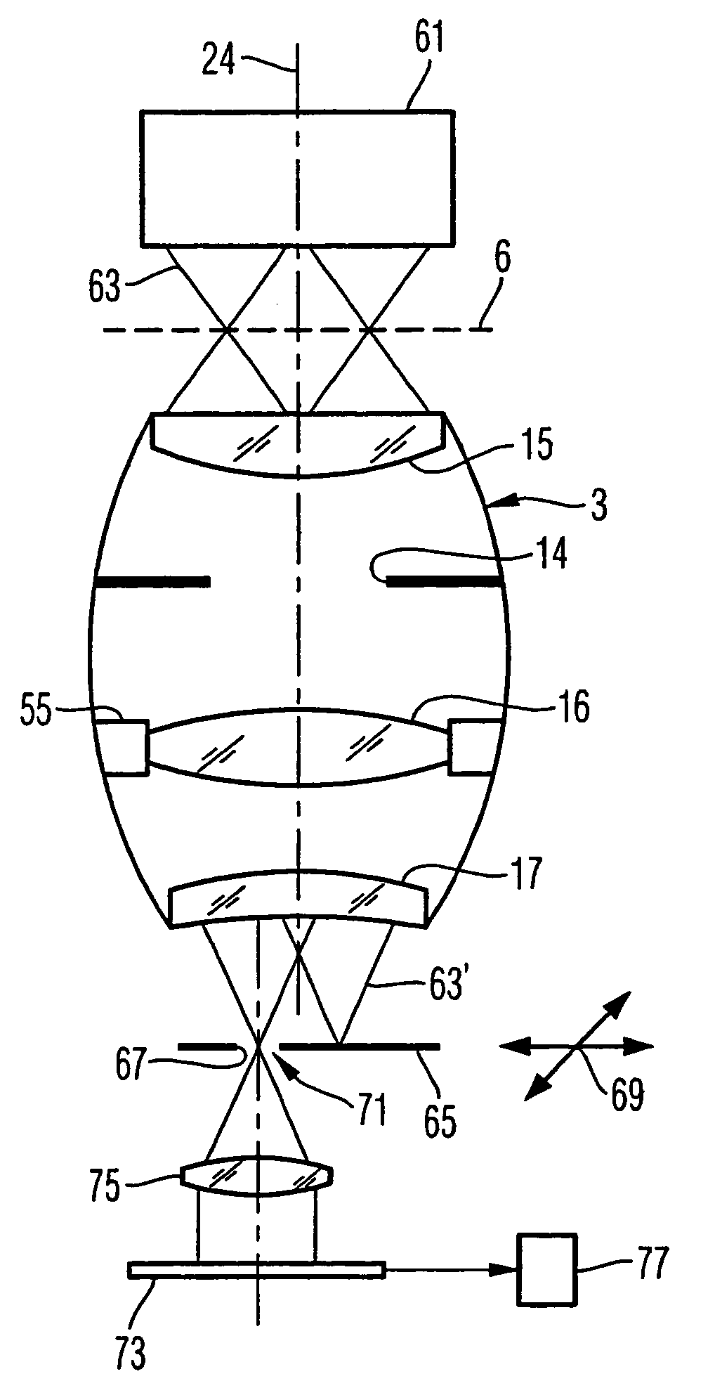
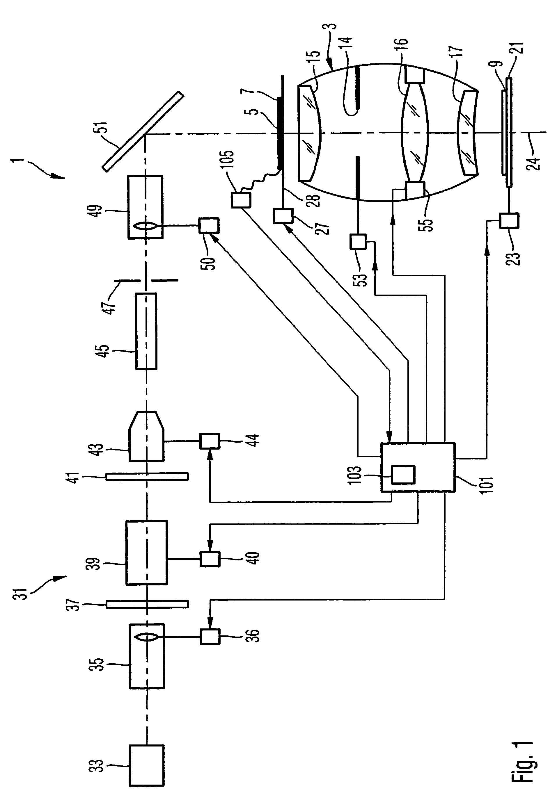
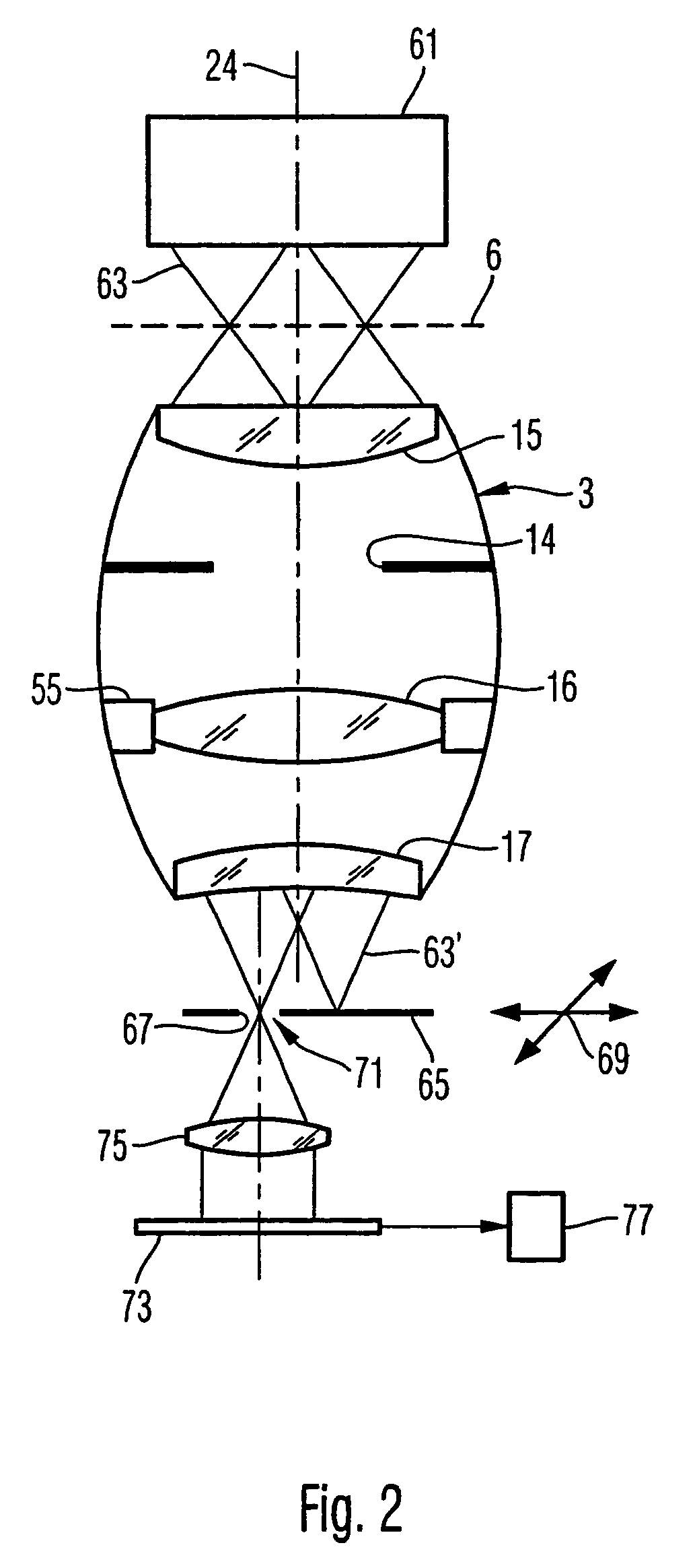
[0033]FIG. 1 schematically illustrates a projection exposure system 1. The projection exposure system 1 comprises a projection optical system 3 for imaging a patterning structure 5 provided on a reticle 7 onto a wafer 9. The patterning structure 5 is disposed in an object plane of the projection optical system 3, and a surface of the wafer 9 is disposed in an image plane of the projection optical system 3.
[0034]FIG. 1 shows a very schematic representation of the projection optical system 3 by indicating only three lenses 15, 16 and 17 and an aperture stop 14. The projection optical system 3 may be of a liquid-immersion type where...
PUM
 Abstract
Description
Claims
Application Information
 - R&D
- Intellectual Property
- Life Sciences
- Materials
- Tech Scout
- Unparalleled Data Quality
- Higher Quality Content
- 60% Fewer Hallucinations
Browse by: Latest US Patents, China's latest patents, Technical Efficacy Thesaurus, Application Domain, Technology Topic, Popular Technical Reports.
© 2025 PatSnap. All rights reserved.Legal|Privacy policy|Modern Slavery Act Transparency Statement|Sitemap|About US| Contact US: help@patsnap.com