Distributed element generator, method of generating distributed elements and an electronic design automation tool employing the same

a technology of distributed elements and generators, applied in the field of electronic design automation, can solve problems such as physical largeness and bad approximation

Active Publication Date: 2009-09-29
TEXAS INSTR INC
View PDF7 Cites 11 Cited by
  • Summary
  • Abstract
  • Description
  • Claims
  • Application Information

AI Technical Summary

Problems solved by technology

The device models may contain accurate parasitic information for the device itself, but do not account for the interactions afforded by its surroundings since its environment is usually unique and therefore not known at the time that the models were developed.
This approach provides an approximation to the reality of the silicon layout and can turn out to be a bad approximation, especially as device operating frequencies increase.
This is particularly true in devices that are physically large.

Method used


Image

  • Distributed element generator, method of generating distributed elements and an electronic design automation tool employing the same
  • Distributed element generator, method of generating distributed elements and an electronic design automation tool employing the same
  • Distributed element generator, method of generating distributed elements and an electronic design automation tool employing the same

Examples


Embodiment Construction

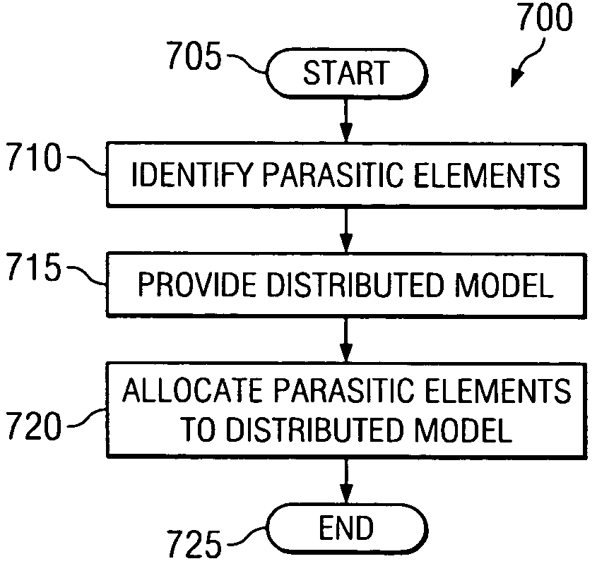
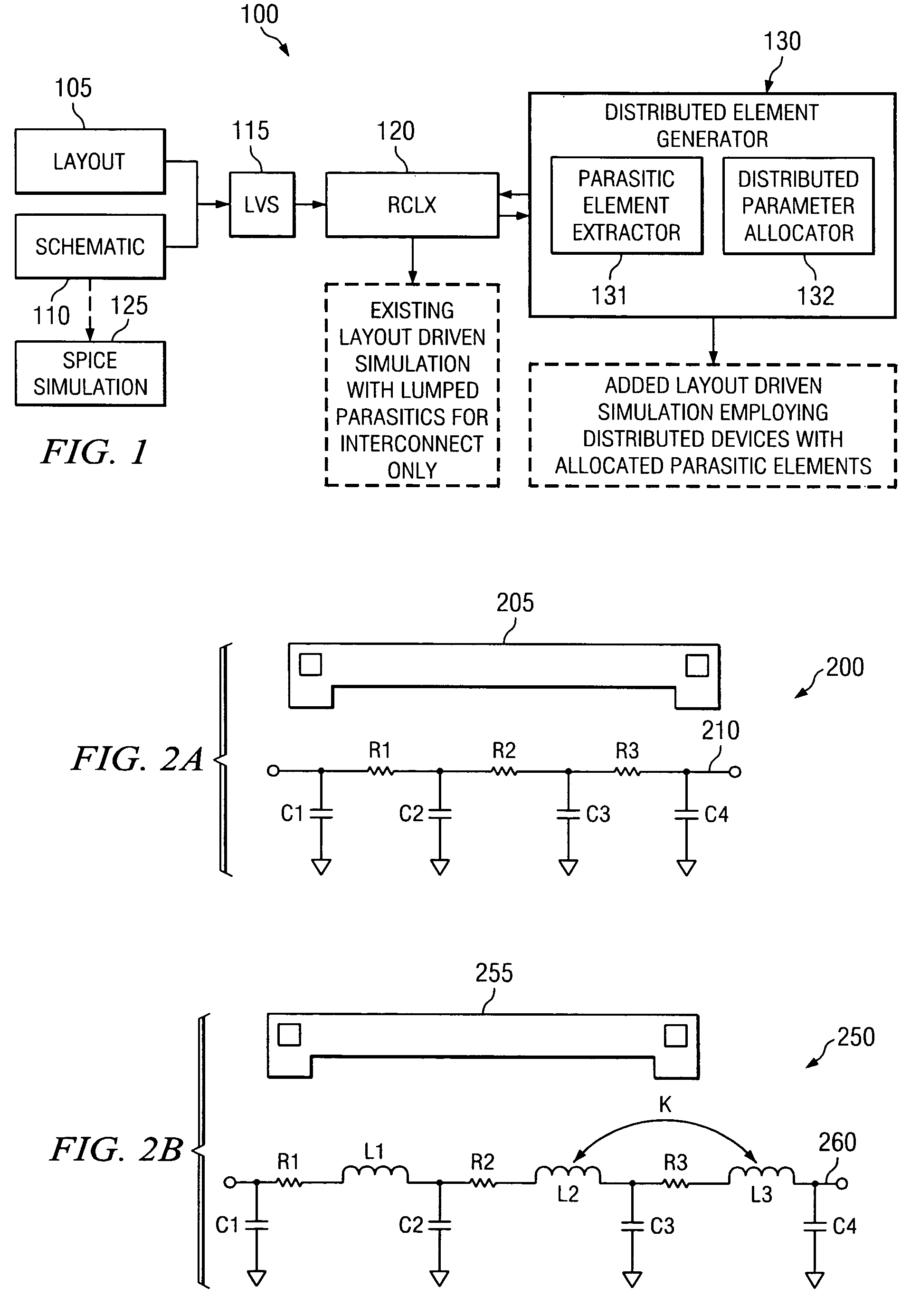
[0018]Referring initially to FIG. 1, illustrated is a block diagram of an embodiment of an electronic design automation tool, generally designated 100, constructed in accordance with the principles of the present invention. The electronic design automation tool 100 includes a layout module 105, a schematic module 110, a layout versus schematic (LVS) module 115, a resistance-capacitance-inductance extraction (RCLX) module 120, a Simulation Program with Integrated Circuit Emphasis (SPICE) module 125 and a distributed element generator 130.

[0019]In the illustrated embodiment, the layout module 105, the schematic module 110, the LVS module 115 and the RCLX module 120 are existing modules as may be associated with an existing electronic design automation tool (e.g., Assura RCX, a Cadence tool). The layout and schematic modules 105, 110 provide layout and schematic information specific to a particular integrated circuit. The LVS module 115 verifies that the layout represents the schematic...


PUM


Abstract

The present invention provides a distributed element generator for use with an electronic design automation tool. In one embodiment, the distributed element generator includes a parasitic element extractor configured to identify parasitic elements associated with a passive integrated circuit device having a surrounding layout environment. Additionally, the distributed element generator also includes a distributed parameter allocator coupled to the parasitic element extractor and configured to provide a distributed model of the passive integrated circuit device and allocate the parasitic elements within the distributed model based on the surrounding layout environment.

Description

TECHNICAL FIELD OF THE INVENTION[0001]The present invention is directed, in general, to electronic design automation and, more specifically, to a distributed element generator, a method of generating distributed elements and an electronic design automation tool employing the generator or the method.BACKGROUND OF THE INVENTION[0002]The product development cycle is under constant pressure to decrease cycle time by moving more quickly from the design phase to properly functioning hardware. The integration of test equipment and electronic design automation and simulation tools typically provides an improvement in product development cycle times. Current models for semiconductor devices do not take into account all of the parasitic elements associated with the way the devices are physically drawn, positioned, and connected.[0003]To address this issue there is a set of electronic design automation tools referred to as “parasitic extractors” that can measure and provide this information fo...

Claims


Application Information

Patent Timeline
Patent Type & Authority Patents(United States)
IPC IPC(8): G06F9/45G06F9/455
CPCG06F17/5036G06F30/367
Inventor COHEN, ISAAC D.KOMAROV, SERGEY F.
Owner TEXAS INSTR INC
Why Eureka
Try Eureka