Semiconductor device and method of manufacturing the same

a technology of semiconductors and semiconductors, applied in the direction of semiconductor devices, basic electric elements, electrical appliances, etc., can solve the problems of inability to obtain a sufficient mobility increase, for example, about two times as much, and the innate characteristics of micro-fabrication are prominen

Active Publication Date: 2009-11-17
KK TOSHIBA
View PDF11 Cites 21 Cited by
  • Summary
  • Abstract
  • Description
  • Claims
  • Application Information

AI Technical Summary

Benefits of technology

[0036]heat-treating the island-like SiGe layer portion left in the n-channel MIS transistor forming region, thereby relaxing lattice strain of the SiGe layer portion;
[0037]selectively etching a surrounding of a region of the SiGe layer, in which a p-channel MIS transistor is to be formed, thereby leaving a portion of the SiGe layer in an island fashion to be long in a channel length direction and short in a channel width direction, thereby relaxing lattice strain in the channel width direction and maintaining the uniaxial compression strain in a channel length direction in the SiGe layer;
[0043]heat-treating the island-like SiGe layer portion left in the n-channel MIS transistor forming region, thereby relaxing lattice strain of the SiGe layer portion;
[0044]selectively etching a surrounding of a region of the SiGe layer, in which a p-channel MIS transistor is to be formed, thereby leaving a portion of the SiGe layer in an island fashion to be long in a channel length direction and short in a channel width direction, thereby relaxing lattice strain in the channel width direction and maintaining the uniaxial compression strain in a channel length direction in the SiGe layer;
[0050]selectively etching the SiGe layer, thereby leaving a portion of the SiGe layer in an island fashion in each of the n-channel MIS transistor forming region and p-channel MIS transistor forming region, to be long in a channel length direction and short in a channel width direction, thereby relaxing lattice strain in the channel width direction and maintaining the uniaxial compression strain in a channel length direction in the SiGe layer;
[0055]selectively etching the SiGe layer, thereby leaving a portion of the SiGe layer in an island fashion in each of the n-channel MIS transistor forming region and p-channel MIS transistor forming region, to be long in a channel length direction and short in a channel width direction, thereby relaxing lattice strain in the channel width direction and maintaining the uniaxial compression strain in a channel length direction in the SiGe layer;

Problems solved by technology

However, at present, where there has been a breakthrough where the gate length is 50 nm or less, various problems innate to the micro-fabrication are becoming prominent.
However, the above-described strain application entails such a drawback that the increase in mobility of pMOSFET is small or substantially none.
However, with a SiGe material having biaxial compression strain, a sufficiently increase in mobility, for example, about two times as much, cannot be obtained if the Ge composition is less than 50%.
Further, the use of a high Ge-concentration channel poses a number of problems in terms of separation formation from that of nMOSFET, crystal defect, leak current, interfacial characteristics of gate insulation film, compatibility with an already-existing Si-LSI process, etc.
As described above, the conventional CMOS structure in which the mobility is improved by lattice strain, still entails such a drawback that a sufficient increase in mobility cannot be obtained for both of the n and p transistors unless the Ge composition is increased and large strain is applied.

Method used


Image

  • Semiconductor device and method of manufacturing the same
  • Semiconductor device and method of manufacturing the same
  • Semiconductor device and method of manufacturing the same

Examples


first embodiment

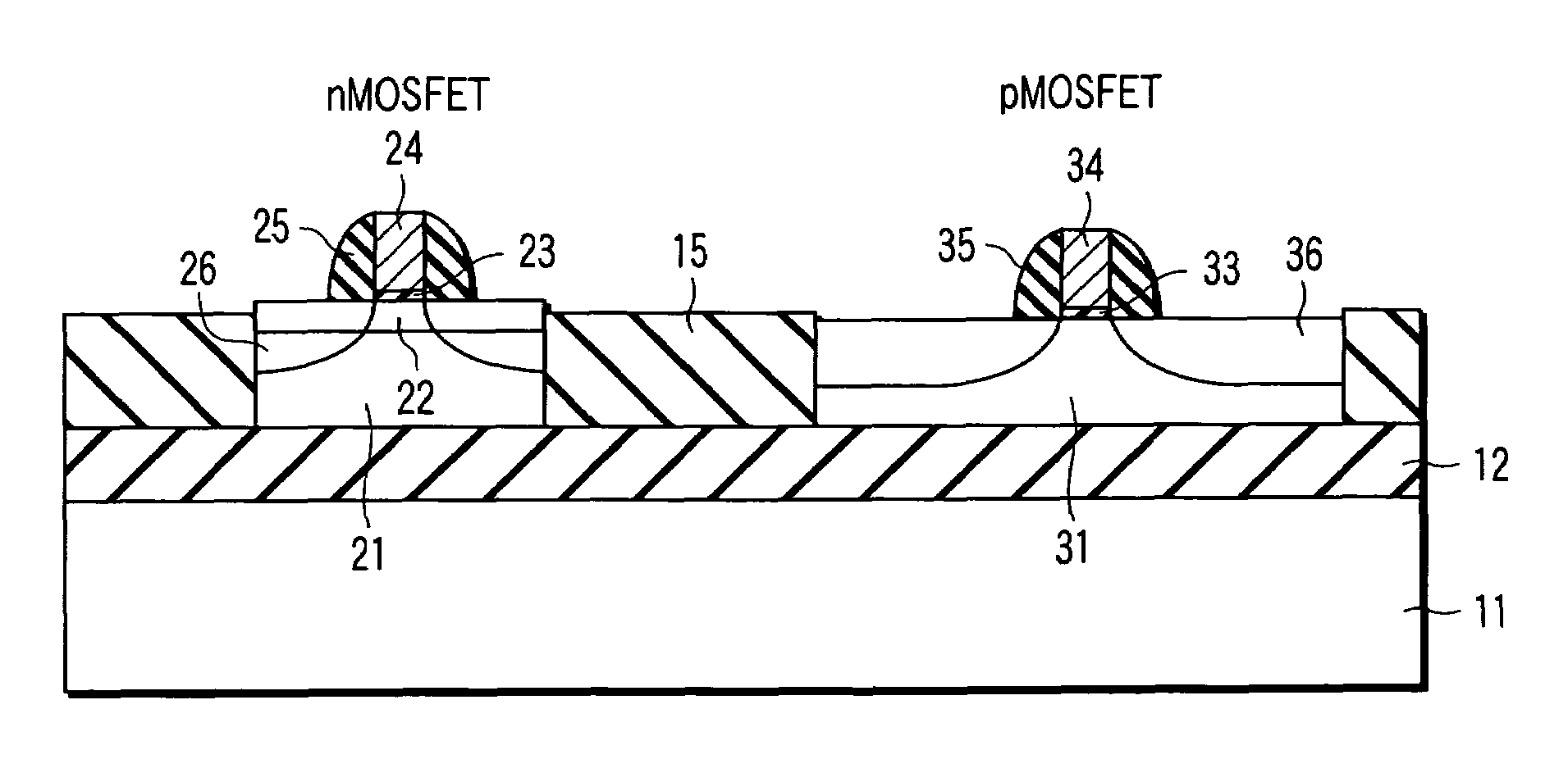
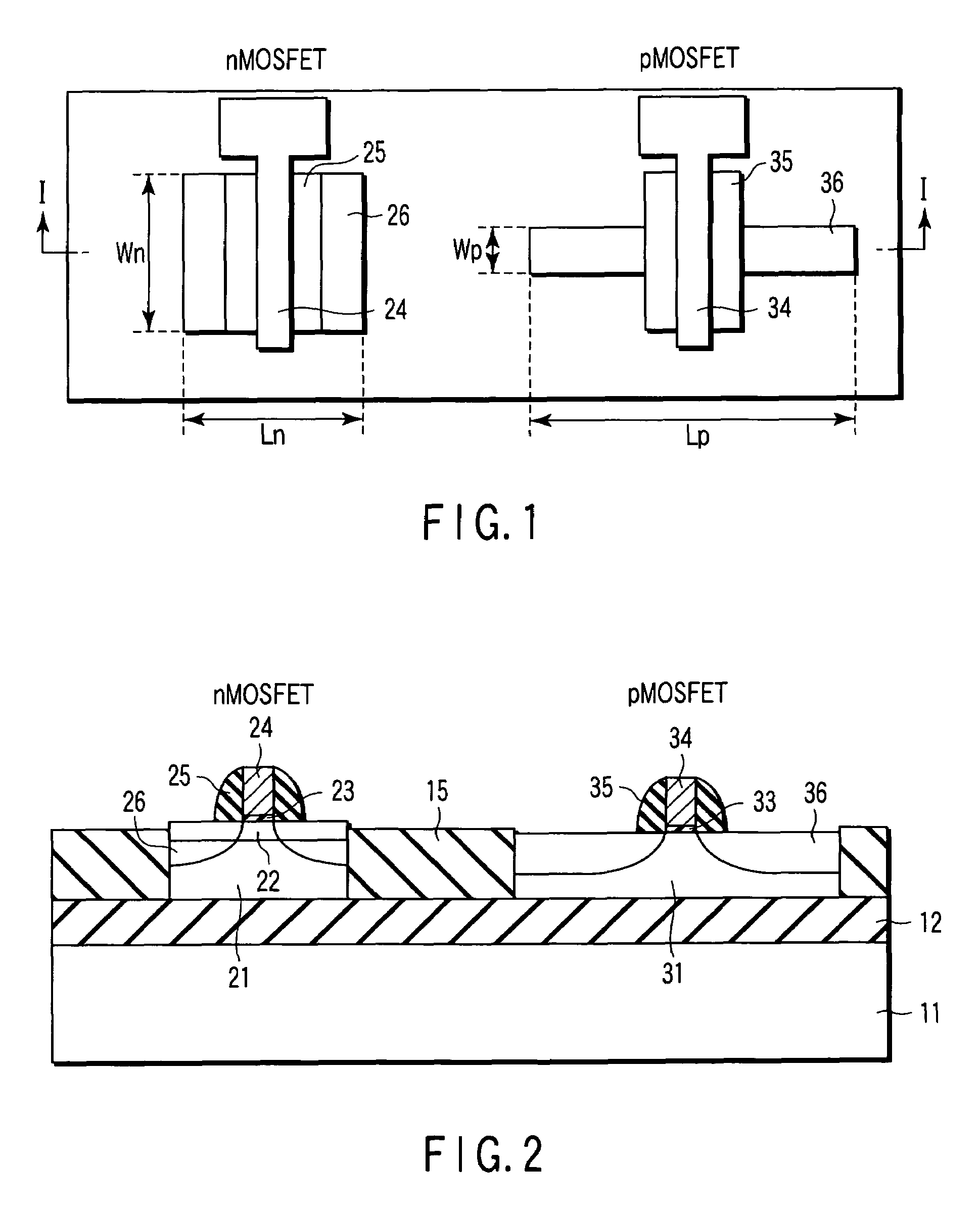
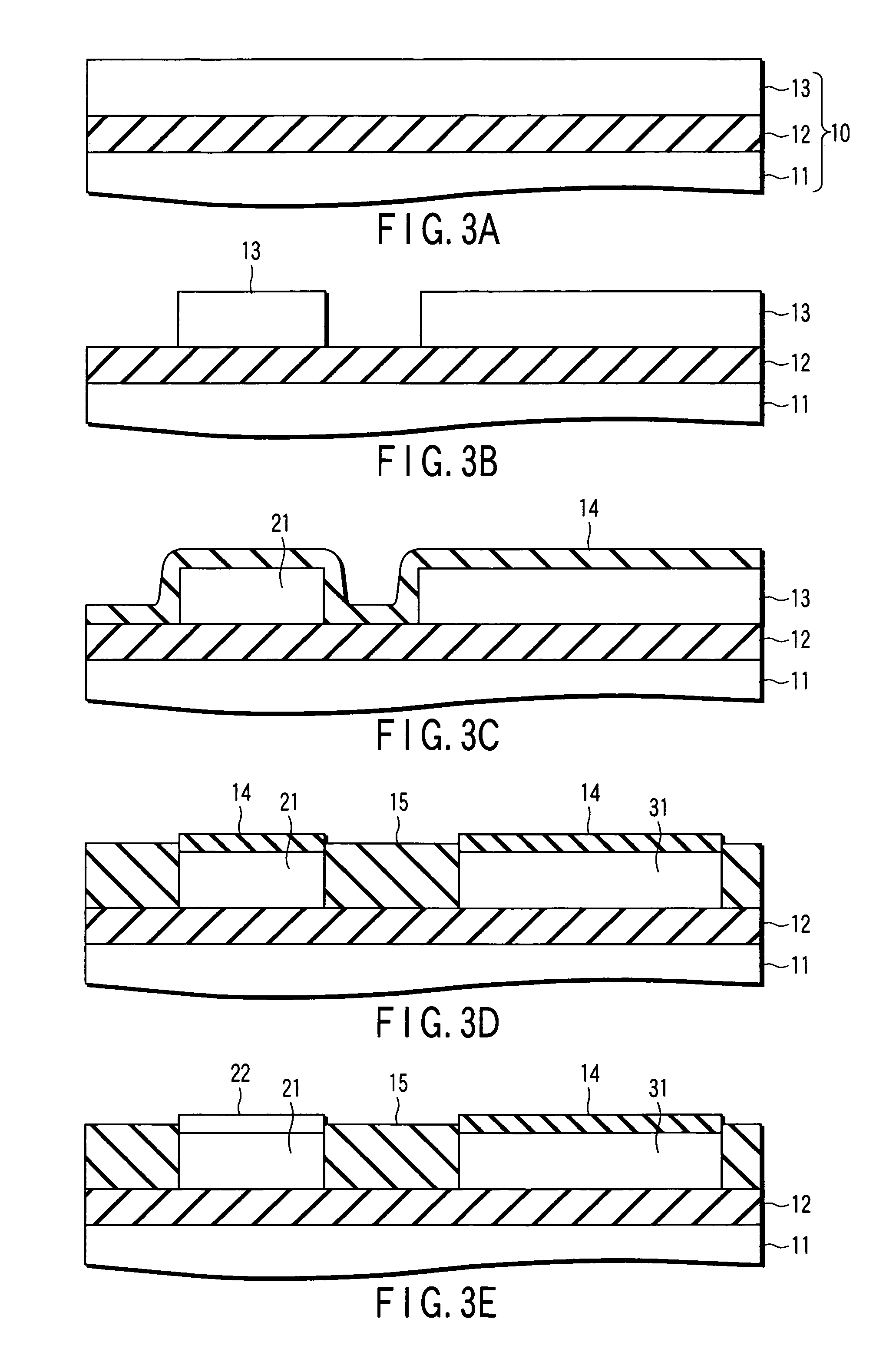
[0072]FIGS. 1 and 2 are diagrams showing a brief structure of a semiconductor device according to the first embodiment of the present invention. FIG. 1 is a plan view of the device, and FIG. 2 is a cross sectional view taken along an arrow I-I shown in FIG. 2.

[0073]As shown in these figures, a Si oxide film (embedded insulating layer) 12 is formed on a Si substrate 11. A lattice-relaxed SiGe layer 21 is formed on a part of the Si oxide film 12, and a strained Si layer 22 is formed on the SiGe layer 21. An nMOSFET is formed on the strained Si layer 22. That is, a gate electrode 24 is formed via a gate insulating film 23 on the strained Si layer 22. A gate sidewall insulating film 25 is formed on each of the sidewalls of the gate electrode 24, and further a source-drain region 26 is formed on the strained Si layer 22.

[0074]A strained SiGe layer 31 is formed on a part of the Si oxide film 12 to interpose an element separation insulating film 15 between the layer 31 itself and the SiGe ...

second embodiment

[0091]FIG. 5 is a cross sectional view showing a brief structure of a CMOS-type semiconductor device according to the second embodiment of the present invention. The same structural elements as those shown in FIG. 2 are designated by the same reference numerals, and the detailed explanations are not repeated here. The plan view of this embodiment is substantially the same as that of FIG. 1 described above, and therefore it is omitted.

[0092]The point of this embodiment, which is different from that of the first embodiment is that the pMOSFET is formed not by the strained SiGe layer 31 having uniaxial compression strain in the channel length direction, but by the strained Si layer 32 having uniaxial tensile strain in the channel width direction.

[0093]As in the case of the first embodiment, the channel of the nMOSFET is a strained Si layer 22 having biaxial tensile strain and formed by epitaxial growth on the lattice relaxed SiGe layer 21. On the other hand, the pMOSFET has a structure...

third embodiment

[0101]FIGS. 7 and 8 are diagrams showing a brief structure of a semiconductor device according to the third embodiment of the present invention. FIG. 7 is a plan view of the device, and FIG. 8 is a cross sectional view taken along an arrow I-I shown in FIG. 7. The same structural elements as those shown in FIGS. 1 and 2 are designated by the same reference numerals, and the detailed explanations are not repeated here.

[0102]The point of this embodiment, which is different from that of the first embodiment is that the nMOSFET is formed not by the strained Si layer having biaxial tensile strain, but by the strained Si layer 42 having uniaxial tensile strain in the channel width direction.

[0103]That is, the channel of the nMOSFET is made of a strained Si layer 42 having uniaxial tensile strain and formed by epitaxial growth on the strained SiGe layer 41 having uniaxial compression strain. On the other hand, the channel of the pMOSFET is formed of the strained SiGe layer 31 having uniaxi...


PUM


Abstract

A semiconductor device includes an n-channel MIS transistor and a p-channel MIS transistor on a semiconductor layer formed on an insulating layer, in which the channel of the n-channel MIS transistor is formed of a strained Si layer having biaxial tensile strain and the channel of the p-channel MIS transistor is formed of a strained SiGe layer having uniaxial compression strain in the channel length direction.

Description

CROSS-REFERENCE TO RELATED APPLICATIONS[0001]This application is based upon and claims the benefit of priority from prior Japanese Patent Application No. 2005-160525, filed May 31, 2005, the entire contents of which are incorporated herein by reference.BACKGROUND OF THE INVENTION[0002]1. Field of the Invention[0003]The present invention relates to a semiconductor device including an n-channel MIS (metal-insulator semiconductor) transistor and a p-channel MIS transistor formed on the same substrate, as well as a method of manufacturing such a device.[0004]2. Description of the Related Art[0005]The drastic improvements of the performance of CMOS circuits have been achieved by micro-fabricating MOSFET based on the scaling rule. However, at present, where there has been a breakthrough where the gate length is 50 nm or less, various problems innate to the micro-fabrication are becoming prominent. Under these circumstances, it is essential for a further improvement of the performance of t...

Claims


Application Information

Patent Timeline
Patent Type & Authority Patents(United States)
IPC IPC(8): H01L29/06
CPCH01L21/84H01L29/78687H01L29/785H01L21/18H01L21/8234H01L21/28
Inventor IRISAWA, TOSHIFUMINUMATA, TOSHINORITEZUKA, TSUTOMUSUGIYAMA, NAOHARUTAKAGI, SHINICHI
Owner KK TOSHIBA
Why Eureka
Try Eureka