
Superconducting member

a superconducting member and member technology, applied in the direction of superconducting magnets/coils, magnetic bodies, waveguides, etc., can solve the problems of inability to accurately regulate the surface shape of the buffer layer provided on the sapphire substrate, difficult to form a (re)bco film having good superconducting properties, and difficulty in realizing a large thickness of not less than 300 nm

Active Publication Date: 2012-01-31
KK TOSHIBA
View PDF14 Cites 0 Cited by
  • Summary
  • Abstract
  • Description
  • Claims
  • Application Information

AI Technical Summary

Benefits of technology

The present invention relates to a method for preparing a thin (Re)BCO film that can achieve high Jc without cracking. To this end, a thin superconducting oxide film is prepared by providing a specific buffer layer between the substrate and the thin superconducting film, and a superconducting member having a high level of electric power resistance is provided. This results in a high Jc value of not less than 4.1×10⁶ A / cm2 for a thin (Re)BCO film grown on an R face cut sapphire single crystal substrate, which is generally available at low cost through a buffer layer of an oxide to about 1 μm, without cracking.

Problems solved by technology

However, it is very difficult to form an (Re)BCO film having good superconducting properties directly on the sapphire substrate, and, so far as the present inventors know, there is no report about any example of success in forming such films.
In fact, it is known that, due to the nature of the crystal structure, mercury(Hg)-type copper oxides having small concavoconvexes in the CuO network structure is unsuitable for practical use because of their many problems with raw materials and production process used, but on the other hand, by virtue of good superconducting properties, the superconducting transition temperature is high and 100 K or above.
Any technique for accurately regulating the surface shape of the buffer layer provided on the sapphire substrate has not been established yet.
However, it is very difficult to realize an (Re)BCO film having a large thickness of not less than 300 nm and simultaneously possessing excellent crystallinity and excellent superconducting properties.
When this method as such is used, a thick film having a thickness of about 1 μm which exhibits superconducting properties can be prepared, but, when a sapphire substrate is used, it is difficult to provide an Ic (=Jc×film thickness) value of not less than 250 A / cm at a liquid nitrogen temperature.
Further, when this method is applied to form a superconducting layer or a buffer layer on the upper part of an R face sapphire substrate with concavoconvexes having a size of not less than 5 nm, the crystallinity of the superconducting layer and the buffer layer cannot be maintained, making it impossible to provide good superconducting properties in the superconducting layer provided on the buffer layer, not to mention in the superconducting layer provided directly on the substrate.
Up to now, however, since any technique for accurately regulating the surface shape of the buffer layer provided on the sapphire substrate has not been established, it has been very difficult to examine the surface shape of the buffer layer necessary for the superconducting layer provided on the buffer layer.

Method used


Image

  • Superconducting member
  • Superconducting member
  • Superconducting member

Examples


examples

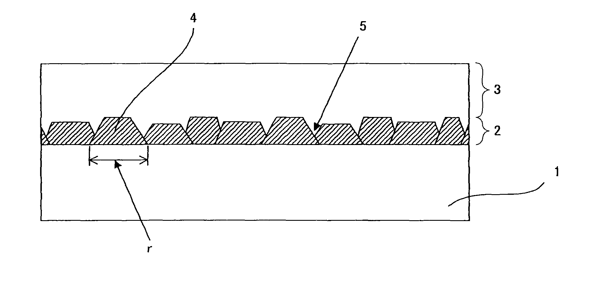
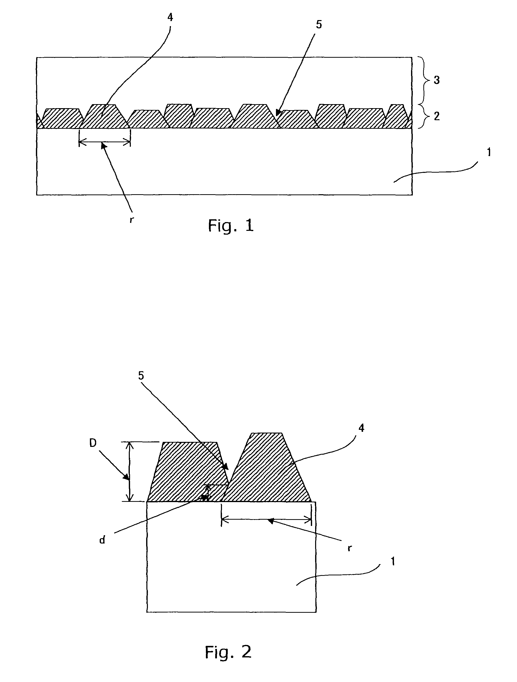
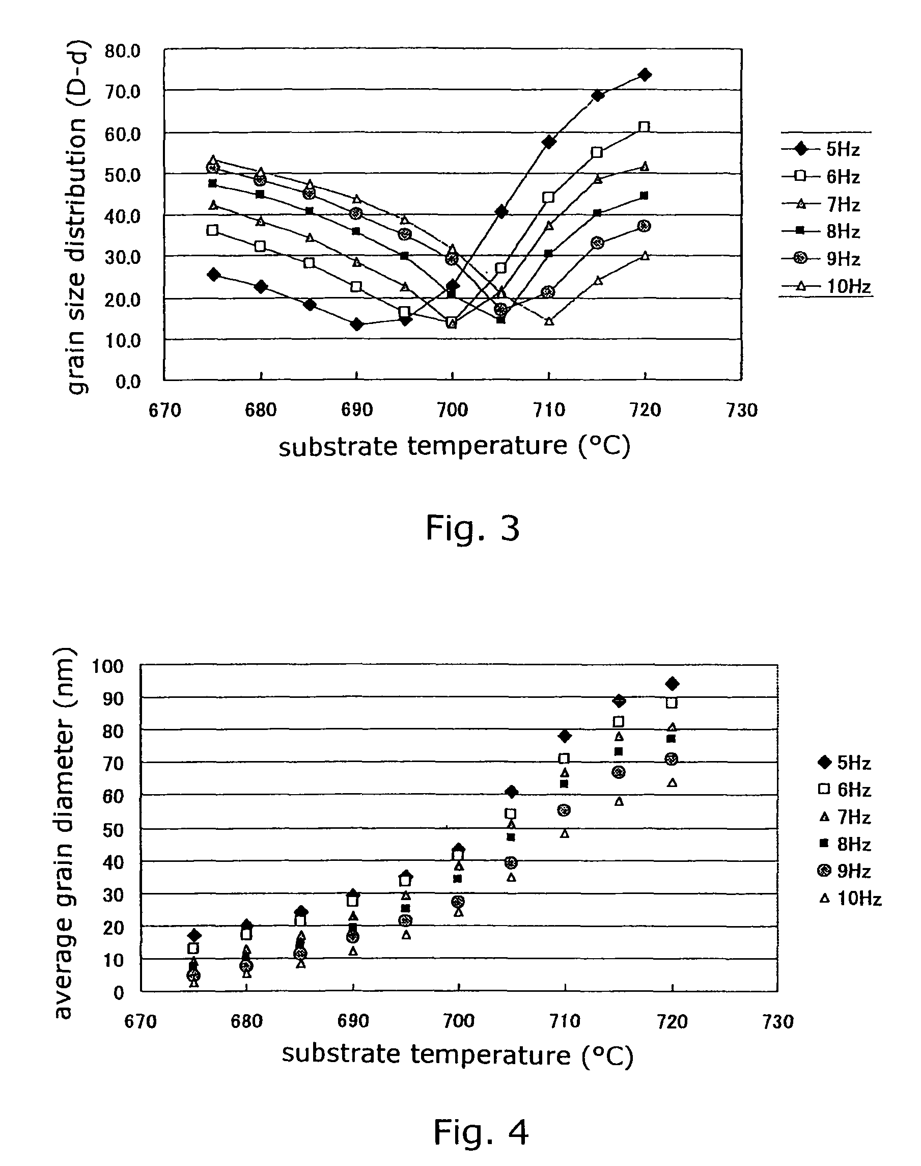
[0036]In relationships shown in FIGS. 3 and 4, buffer layers were formed by regulating the grain diameter r [nm] of grain lumps of an oxide constituting a buffer layer 2 and the distribution of the grain diameter for various buffer layer materials. A 500 nm-thick thin YBCO film was grown on the buffer layers. For the superconducting members thus obtained, the critical current density Jc was measured. The results thus obtained were as shown in Table 2. In Table 2, the grain diameter r of the grain lumps of the buffer layer is expressed in a diameter range. For example, 10 nm≦r≦30 nm means that the grain diameter of not less than 90% of grain lumps which can be confirmed by a sectional TEM image is in the range of 10 nm≦r≦30 nm. The same studies have been made for superconducting layers, i.e., a 500 nm-thick thin YbBCO film and a 500 nm-thick thin NdBCO film different from each other in lattice constant. The results are shown in Tables 3 and 4.

[0037]

TABLE 2Distancebetweennearestneighb...


PUM

PropertyMeasurementUnit
thicknessaaaaaaaaaa
thicknessaaaaaaaaaa
thicknessaaaaaaaaaa

Abstract

This invention provides a thin superconducting oxide film, which can realize a high critical current, and a superconducting member having a high level of electric power resistance. The superconducting member comprises a sapphire R face substrate, a buffer layer formed of grain lumps of an oxide provided on the sapphire R face substrate, and a superconducting layer provided on the buffer layer. The nearest neighbor distance between oxygen atoms in the oxide and the grain diameter of grain lumps of the oxide have been specified. The superconducting member can be used as a member for superconducting filters.

Description

CROSS-REFERENCE TO RELATED APPLICATIONS[0001]This application is based upon and claims the benefit of priority from the prior Japanese Patent Applications No. 243848 / 2007, filed on Sep. 20, 2007; the entire contents of which are incorporated herein by reference.BACKGROUND OF THE INVENTION[0002]1. Field of the Invention[0003]The present invention relates to a superconducting member. More particularly, the present invention relates to a superconducting member comprising a super conducting material in a part of a component which can transmit a high frequency electric power having a predetermined frequency on the order of MHz or more selectively and with low loss.[0004]2. Background Art[0005]Superconducting filters can realize the production of a small-size resonator having a small material loss and a high Q value. Consequently, steep skirt properties unattainable by the conventional filter can be realized, and, hence, efforts have been made to put high frequency filters on the order of...

Claims


Application Information

Patent Timeline
Patent Type & Authority Patents(United States)
IPC IPC(8): H01L39/24H01P1/203H01B12/02C23C14/08
CPCH01L39/2461Y10S505/703Y10T428/25H10N60/0632
Inventor NAKAYAMA, KOHEIYAMAZAKI, MUTSUKI
Owner KK TOSHIBA
Learn More