Non-volatile memory device and method of operating the same

a non-volatile memory and non-volatile technology, applied in static storage, digital storage, instruments, etc., can solve the problems of disturbance, disadvantage of flash memory in terms of higher speed, etc., and achieve the effect of sufficient boosting

Inactive Publication Date: 2011-01-04
SK HYNIX INC
View PDF14 Cites 6 Cited by
  • Summary
  • Abstract
  • Description
  • Claims
  • Application Information

AI Technical Summary

Benefits of technology

[0013]The present invention is directed towards a non-volatile memory device and a method of operating the same, in which boosting can be generated sufficiently by applying a pass voltage, which is changed according to a degree that a memory cell connected to a unselected word line is programmed at the time of a program operation.

Problems solved by technology

The NAND flash memory is disadvantageous in terms of higher speed due to a low cell current, but is advantageous in terms of higher integration since a plurality of cells shares one contact.
Further, disturbance may be caused since boosting is not sufficient.

Method used


Image

  • Non-volatile memory device and method of operating the same
  • Non-volatile memory device and method of operating the same
  • Non-volatile memory device and method of operating the same

Examples


Embodiment Construction

[0030]Specific embodiments according to the present invention will be described with reference to the accompanying drawings. However, the present invention is not limited to the disclosed embodiments, but may be implemented in various manners. The embodiments are provided to complete the disclosure of the present invention and to allow those having ordinary skill in the art to understand the present invention. The present invention is defined by the scope of the claims.

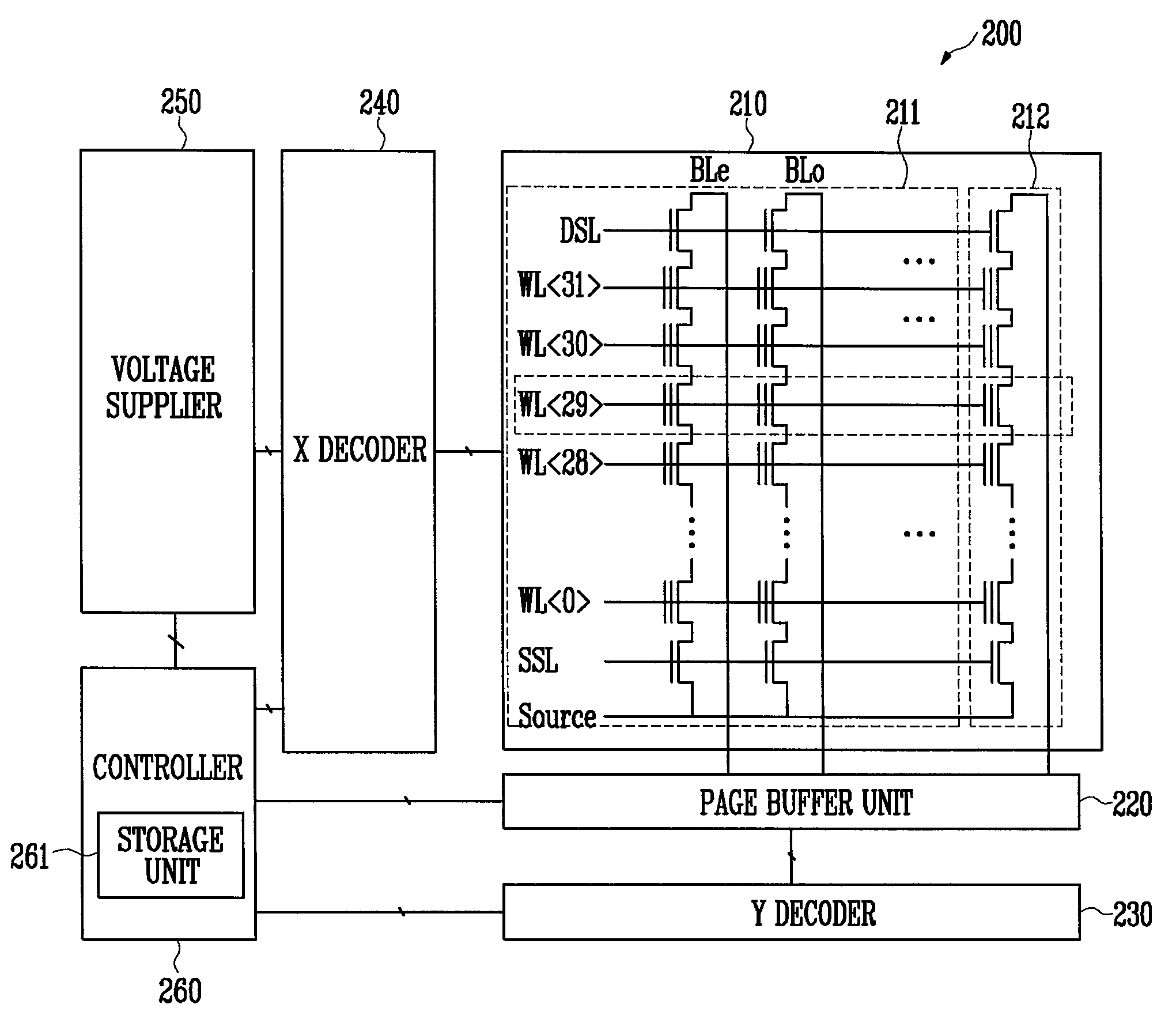
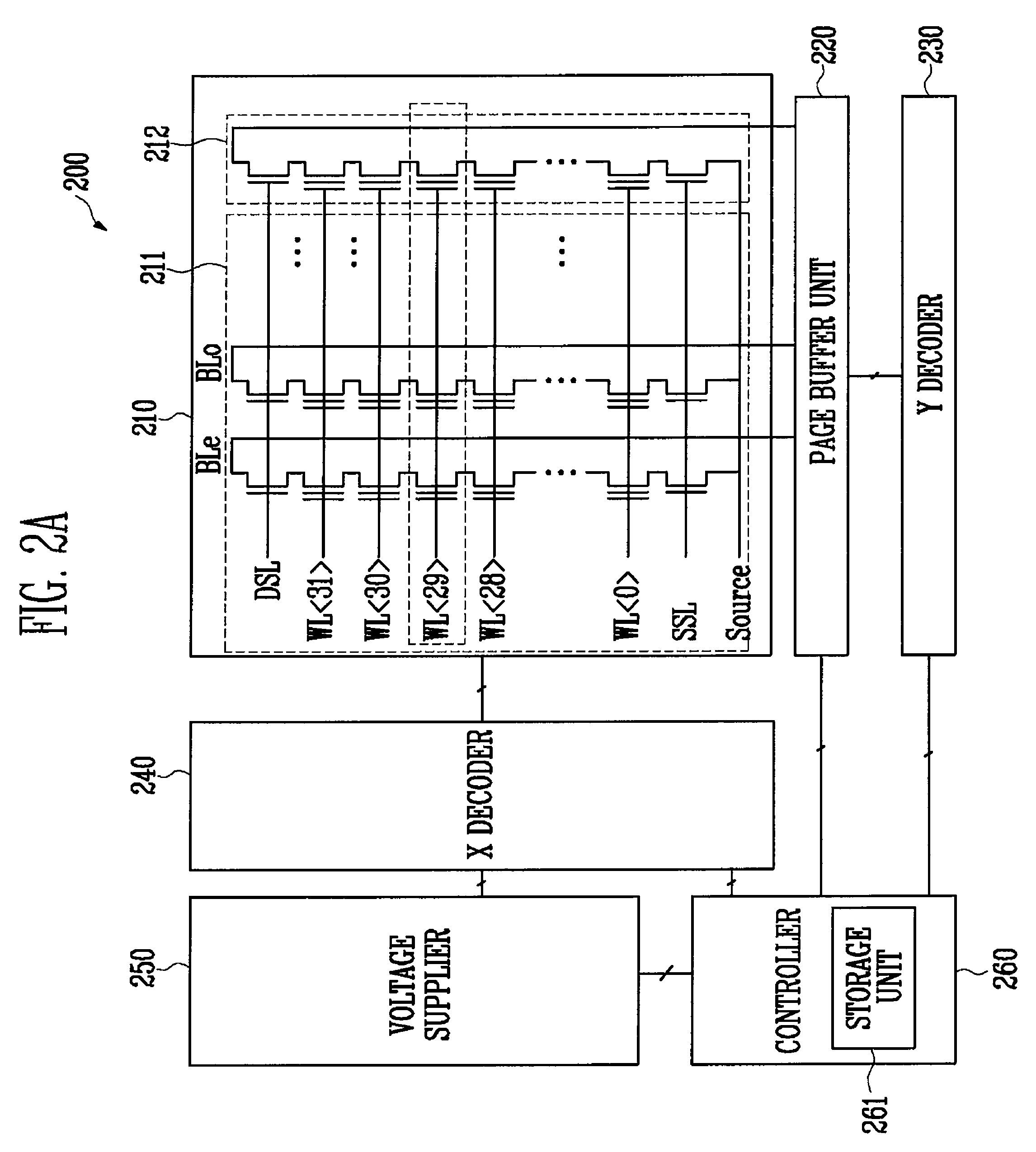
[0031]FIG. 2A is a block diagram showing the structure of a flash memory device according to an embodiment of the present invention.

[0032]Referring to FIG. 2A, a flash memory device 200 according to an embodiment of the present invention includes a memory cell array 210, a page buffer unit 220, a Y decoder 230, an X decoder 240, a voltage supplier 250, and a controller 260.

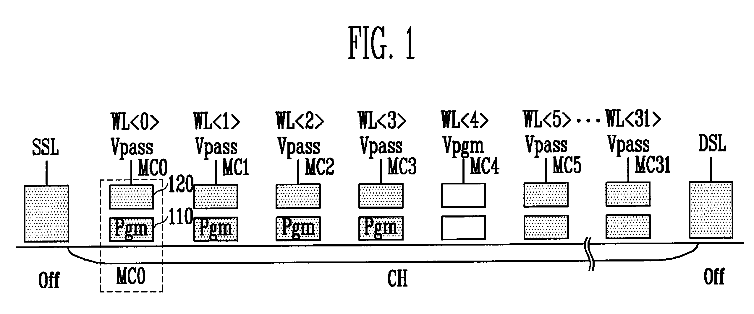
[0033]The memory cell array 210 includes a main cell unit 211 having memory cells for data storage and a flag cell unit 212 having flag cells. The ...


PUM


Abstract

A non-volatile memory device includes a memory cell array and a controller. The memory cell array includes memory cells for data storage and a plurality of flag cells. The flag cells indicate program states of the memory cells for each of a plurality of word lines. The controller determines the program states of the memory cells by employing the flag cells and controls a pass voltage provided to a corresponding word line according to the determined program states.

Description

CROSS-REFERENCES TO RELATED APPLICATIONS[0001]The present application claims priority to Korean patent application number 10-2007-140188, filed on Dec. 28, 2007, which is incorporated by reference in its entirety.BACKGROUND OF THE INVENTION[0002]The present invention relates to an operation of a non-volatile memory device and, more particularly, to a non-volatile memory device and a method of operating the same, in which a pass voltage is supplied depending on the characteristics of word lines.[0003]Semiconductor memory devices can be classified into volatile memory devices which do not retain data, such as dynamic random access memory (DRAM) and static random access memory (SRAM), and non-volatile memory devices which retain data after the data is input.[0004]Recently, there has been an increasing demand for flash memory into which data can be electrically input or from which data can be electrically erased. Flash memory is a device that can be electrically erased at a high speed w...

Claims


Application Information

Patent Timeline
Patent Type & Authority Patents(United States)
IPC IPC(8): G11C16/06G11C16/04
CPCG11C16/10G11C16/26G11C16/0483G11C16/12G11C16/34
Inventor KIM, YOU SUNGSHIN, TAE HO
Owner SK HYNIX INC
Why Eureka
Try Eureka