Non-volatile memory device

a memory device and non-volatile technology, applied in static storage, digital storage, instruments, etc., can solve the problems of difficulty in controlling the interval between the threshold voltage and the width of the threshold voltage distribution, and achieve the effect of increasing the number of word lines and augmenting storage capacity

Active Publication Date: 2010-09-07
SK HYNIX INC
View PDF9 Cites 7 Cited by
  • Summary
  • Abstract
  • Description
  • Claims
  • Application Information

AI Technical Summary

Benefits of technology

[0024]It is a feature of the present invention to provide a non-volatile memory device for increasing a number of word lines and a storage capacity using a multi level cell.
[0032]As described above, a non-volatile memory device of the present invention increases the number of word lines in a memory cell array and augments storage capacity using a multi level cell. In addition, the non-volatile memory device addresses a problem of self-boosting not being adequately generated due to the increased number of word lines.

Problems solved by technology

It is difficult to control the interval between the threshold voltages and the width of the threshold voltage distributions as the number of data bits is increased.
However, this method may be used only if problems such as those related to a size of a memory device chip and those related to voltage control for a cell boosting operation in a program operation are solved.

Method used


Image

  • Non-volatile memory device
  • Non-volatile memory device
  • Non-volatile memory device

Examples


Embodiment Construction

[0039]Hereinafter, the preferred embodiments of the present invention will be explained in more detail with reference to the accompanying drawings.

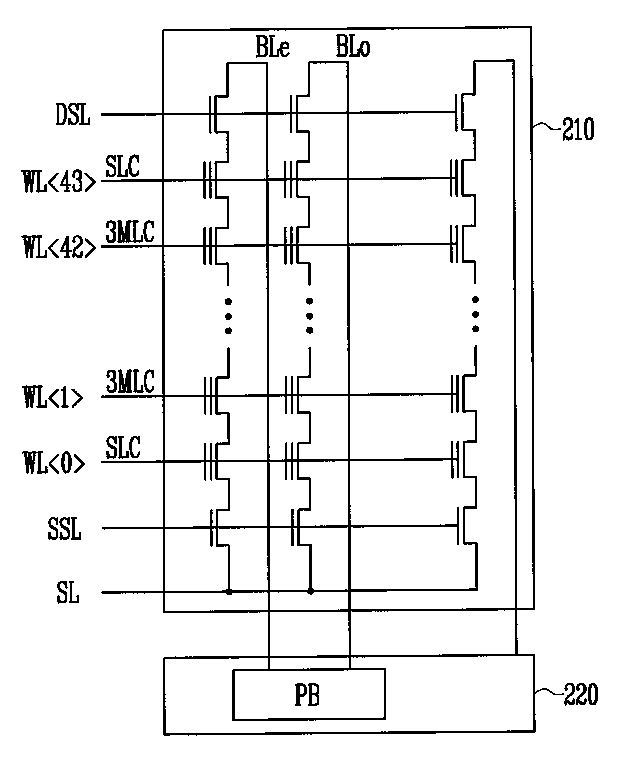
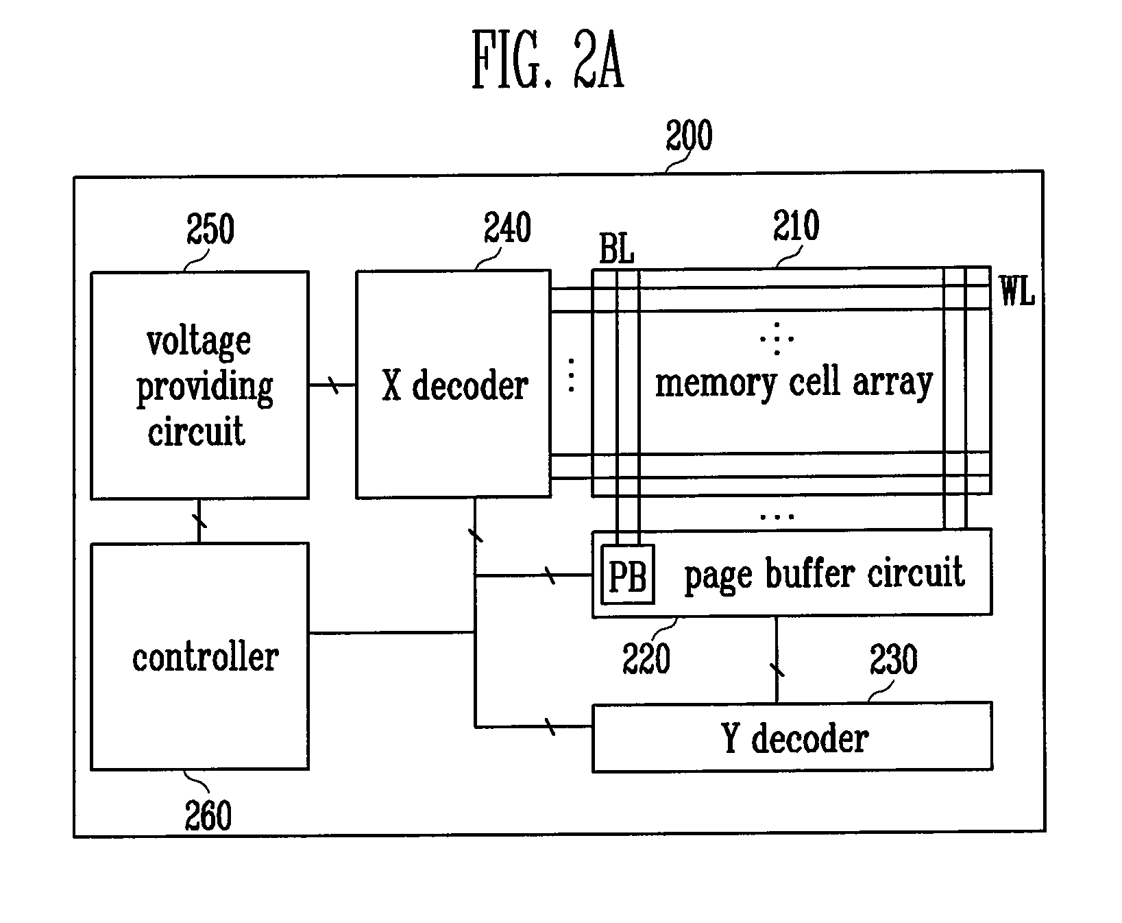
[0040]FIG. 2A is a block diagram illustrating a flash memory device.

[0041]In FIG. 2A, the flash memory device 200 includes a memory cell array 210, a page buffer circuit 220, a Y decoder 230, an X decoder 240, a voltage providing circuit 250 and a controller 260.

[0042]The memory cell array 210 has cell strings in which memory cells for storing data are coupled in series. Each of the cell strings is coupled to a corresponding bit line BL. In addition, gates of the memory cells are coupled to corresponding word lines WL in a direction vertical to the bit lines BL.

[0043]The page buffer circuit 220 includes a plurality of page buffers PB coupled to the bit lines BL of the memory cell array 210. Each of the page buffers PB temporarily stores data to be programmed in a selected memory cell and then transmits the stored data to the memory cell t...


PUM


Abstract

A non-volatile memory device increases a number of word lines and a storage capacity using a multi level cell. The non-volatile memory device addresses a problem of self-boosting not being adequately generated due to the increased number of word lines. The non-volatile memory device includes a memory cell array configured to have first memory cells for storing first bit information coupled to third word lines except a first word line adjacent to a drain select line and a second word line adjacent to a source select line, and second memory cells coupled to the first word line and the second word line. The second memory cells store second bit information that is smaller than the first bit information.

Description

CROSS-REFERENCE TO RELATED APPLICATIONS[0001]This application claims priority from Korean Patent Application No. 10-2008-0023839, filed on Mar. 14, 2008, the contents of which are incorporated herein by reference in its entirety.BACKGROUND OF THE INVENTION[0002]The present invention relates to a non-volatile memory device. More particularly, the present invention relates to a non-volatile memory device for increasing storage capacity of data by augmenting a number of word lines of a memory device.[0003]Generally, a flash memory device such as a non-volatile memory device is divided into categories of an NAND flash memory device and an NOR flash memory device.[0004]In the NOR flash memory, each of the memory cells is connected independently to a bit line and a word line. Thus, the NOR flash memory has an excellent random access time. In the NAND flash memory, only one contact is required for one cell string because memory cells are connected in series in the cell string. Thus, the NA...

Claims


Application Information

Patent Timeline
Patent Type & Authority Patents(United States)
IPC IPC(8): G11C16/00
CPCG11C11/5621G11C16/0483G11C2211/5641H10B63/80
Inventor KIM, YOU SUNGRHO, JUN RYE
Owner SK HYNIX INC
Why Eureka
Try Eureka