Methods and apparatuses for double sided dark reference pixel row-wise dark level non-uniformity compensation in image signals

a row-wise, non-uniform compensation and image signal technology, applied in the field of image signals, can solve the problems of horizontal shading across the array, distortion of the resulting digital image, and physical non-uniformity of the array becoming more prominen

Active Publication Date: 2011-04-12
APTINA IMAGING CORP
View PDF28 Cites 6 Cited by
  • Summary
  • Abstract
  • Description
  • Claims
  • Application Information

AI Technical Summary

Problems solved by technology

However, various noise sources can affect individual pixel outputs and thus distort the resulting digital image.
As CMOS pixel arrays increase in size to obtain higher resolution, the physical non-uniformity of the arrays becomes more prominent.
One issue occurring in higher resolution imaging sensors, such as, for example, eight or more megapixel sensors, is row-wise dark level non-uniformity that increases across the pixel array as the column number increases, causing a horizontal shading across the array.

Method used


Image

  • Methods and apparatuses for double sided dark reference pixel row-wise dark level non-uniformity compensation in image signals
  • Methods and apparatuses for double sided dark reference pixel row-wise dark level non-uniformity compensation in image signals
  • Methods and apparatuses for double sided dark reference pixel row-wise dark level non-uniformity compensation in image signals

Examples


Embodiment Construction

[0018]In the following detailed description, reference is made to the accompanying drawings which form a part hereof, and in which is shown by way of illustration specific embodiments that may be practiced. These embodiments are described in sufficient detail to enable those of ordinary skill in the art to make and use them, and it is to be understood that structural, logical, or procedural changes may be made to the specific embodiments disclosed.

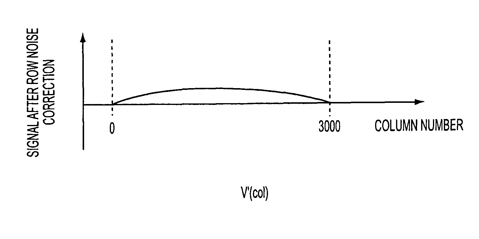
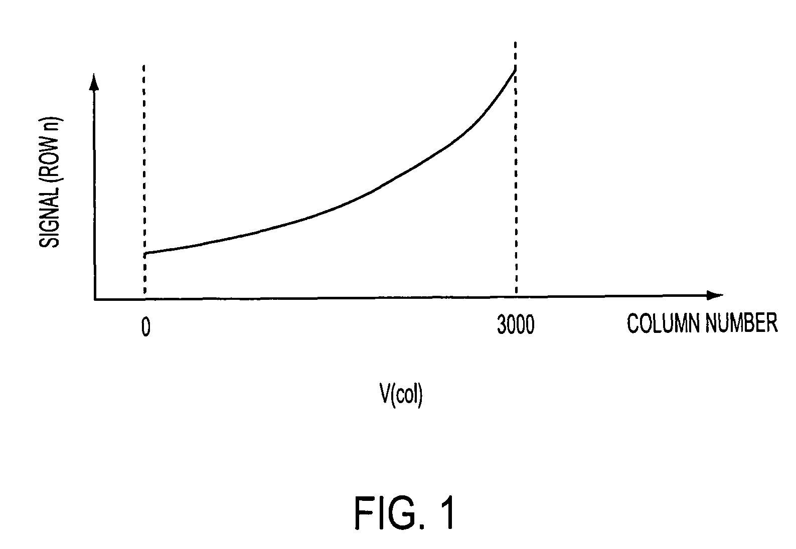
[0019]Row-wise dark level non-uniformity has two components, amplitude and phase. When row-wise dark level non-uniformity compensation is applied, if a pixel signal value being corrected and a dark reference value are well correlated (i.e., have the same phase), dark level non-uniformity will be suppressed. When row-wise dark level non-uniformity compensation is applied, if the pixel signal value being corrected and the dark reference value are not well correlated (i.e., do not have the same phase), dark level non-uniformity may be undesir...


PUM


Abstract

Methods and apparatuses for row-wise dark level non-uniformity compensation of imaging sensor pixel signals. A column dependent dark reference value is determined as one of a linear and parabolic function of signal values from two areas of dark reference pixels and a column location and then used for dark level non-uniformity compensation of signal values from imaging pixels.

Description

FIELD OF THE INVENTION[0001]The embodiments described herein relate generally to imaging devices and, more specifically, to methods and apparatuses for row-wise dark level non-uniformity compensation in image signals from imaging sensors employed in such devices.BACKGROUND OF THE INVENTION[0002]Solid state imaging devices, including charge coupled devices (CCD), complementary metal oxide semiconductor (CMOS) imaging devices, and others, have been used in photo imaging applications. A solid state imaging device circuit includes a focal plane array of pixel cells or pixels as an imaging sensor, each cell including a photosensor, which may be a photogate, photoconductor, a photodiode, or other photosensor having a doped region for accumulating photo-generated charge. For CMOS imaging devices, each pixel has a charge storage region, formed on or in the substrate, which is connected to the gate of an output transistor that is part of a readout circuit. The charge storage region may be co...

Claims


Application Information

Patent Timeline
Patent Type & Authority Patents(United States)
IPC IPC(8): H04N9/64
CPCH04N5/361H04N5/374H04N9/045H04N25/63H04N23/10H04N25/76
Inventor XU, CHENMO, YAOWUYAN, MEI
Owner APTINA IMAGING CORP
Why Eureka
Try Eureka