Diffraction optical element, lighting device, and projector
a technology of optical elements and lighting devices, applied in fixed installations, lighting and heating apparatus, instruments, etc., can solve the problems of image quality reduction and other problems, and achieve the effect of preventing the decrease of light utilization efficiency
- Summary
- Abstract
- Description
- Claims
- Application Information
AI Technical Summary
Benefits of technology
Problems solved by technology
Method used
Image

Examples
first embodiment
Modification of First Embodiment
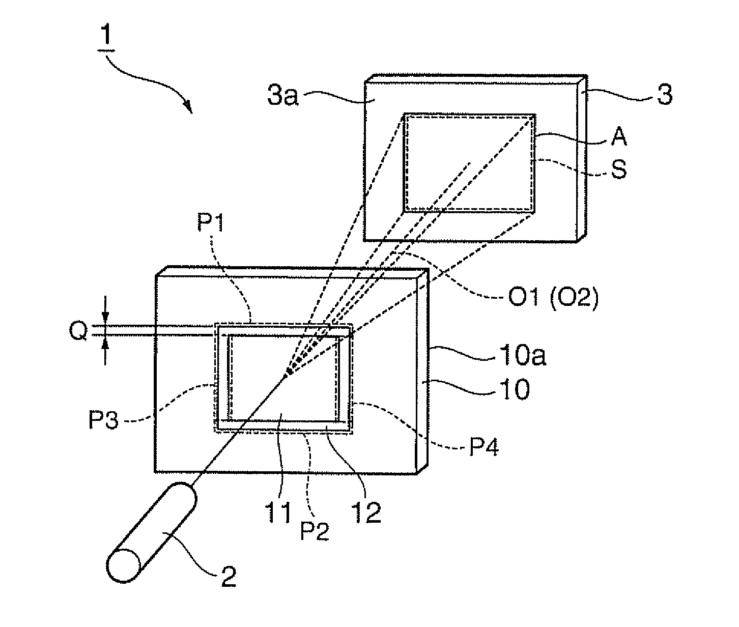
[0082]While the light source device 2 has one light mission unit in the first embodiment shown in FIG. 1, the light source device 2 of a lighting device 15 shown in FIG. 6 may includes a plurality of light emission units 16a, 16b and 16c (three in the example shown in the figure).
[0083]The diffraction optical element 10 included in the lighting device 15 has the first diffraction pattern 11 having a sufficient size for receiving laser beams emitted from the plural light emission units 16a, 16b and 16c. Thus, the laser beam shifted out of the first diffraction pattern 11 due to shift of the diffraction optical element 10 enters the second diffraction pattern 12 to illuminate the illumination area S of the predetermined surface 3a. According to this structure, the size of the first diffraction pattern 11 can be determined according to the positions of the plural light emission units 16a through 16c. Thus, the manufacture cost can be reduced by simplific...
second embodiment
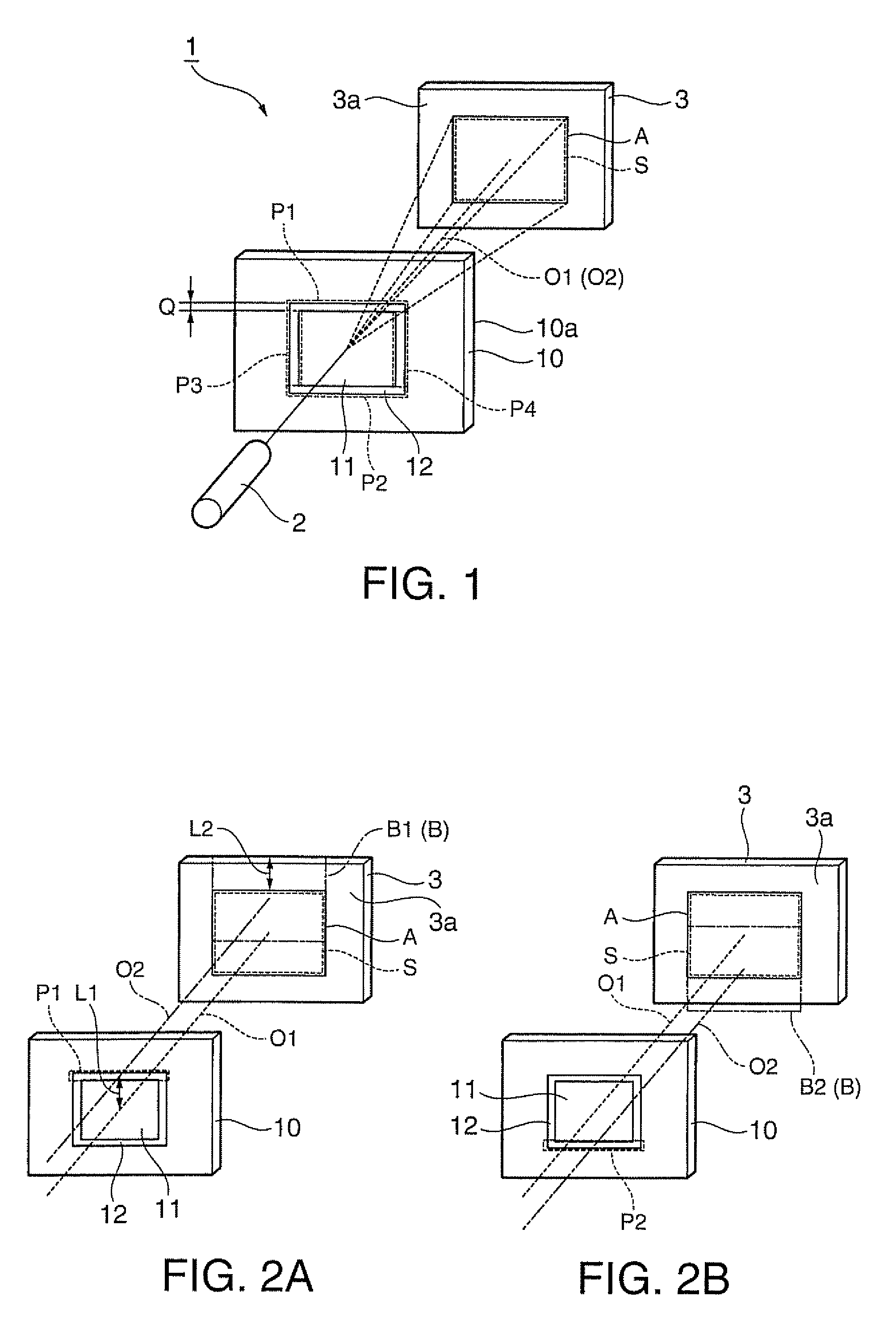
[0086]A second embodiment according to the invention is now described with reference to FIGS. 8 through 10. In the following description of the respective embodiments, similar reference numbers are given to parts having structures similar to those of the parts of the lighting device 1 in the first embodiment, and the same explanation is not repeated.
[0087]A lighting device 20 according to this embodiment is different from the lighting device 1 having the diffraction optical element 10 in the first embodiment in that the lighting device 20 has a second diffraction pattern 27.
[0088]As illustrated in FIG. 8, the second diffraction pattern 27 has three narrow sub diffraction patterns 27a, 27b and 27c disposed in this order from the first diffraction pattern 11. That is, the width Q of the second diffraction pattern 12 of the diffraction optical element 10 in the first embodiment is approximately three times larger than the entering laser beam, but each of widths Q1, Q2 and Q3 of the sub...
third embodiment
[0104]A third embodiment according to the invention is now described with reference to FIG. 11.
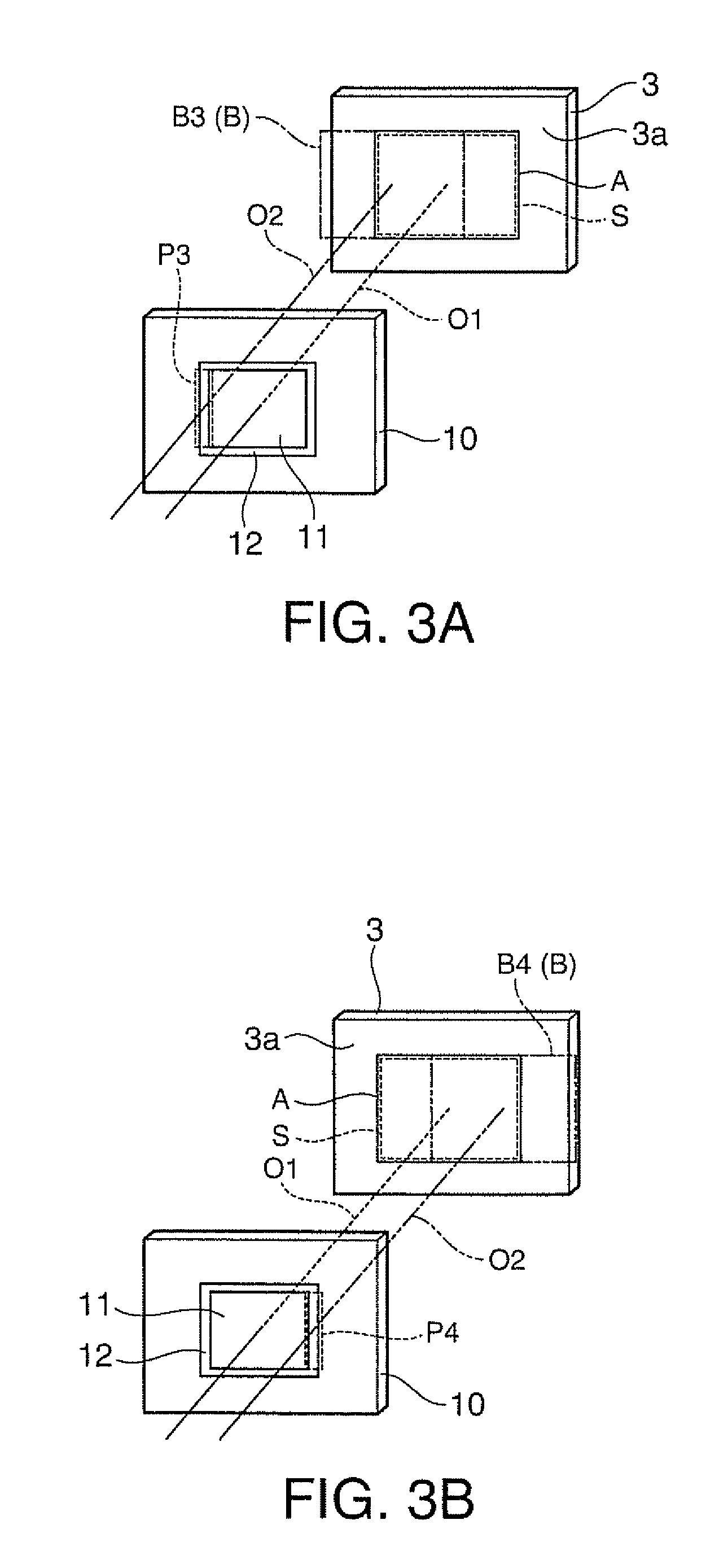
[0105]A lighting device 30 in this embodiment is different from the lighting device 1 in the first embodiment in that a movable member 31 for moving the diffraction optical element 10 is provided.
[0106]The movable member (shift unit) 31 shifts (oscillates) the diffraction optical element 10 on the plane perpendicular to the center axis O2 of laser beam emitted from the light source device 2. More specifically, the movable member 31 reciprocates the diffraction optical element 10 in the direction inclined to an upper end surface 10b of the diffraction optical element 10 at 45 degrees (direction indicated by an arrow w).
[0107]The movable member 31 shifts the diffraction optical element 10 such that the laser beam emitted from the light source device 2 can enter the first diffraction pattern 11 and the second diffraction pattern 12 of the diffraction optical element 10. More specifically, the...
PUM
 Abstract
Description
Claims
Application Information
 - Generate Ideas
- Intellectual Property
- Life Sciences
- Materials
- Tech Scout
- Unparalleled Data Quality
- Higher Quality Content
- 60% Fewer Hallucinations
Browse by: Latest US Patents, China's latest patents, Technical Efficacy Thesaurus, Application Domain, Technology Topic, Popular Technical Reports.
© 2025 PatSnap. All rights reserved.Legal|Privacy policy|Modern Slavery Act Transparency Statement|Sitemap|About US| Contact US: help@patsnap.com