Semiconductor device including a plurality of diffusion layers and diffusion resistance layer

a technology of diffusion resistance layer and semiconductor device, which is applied in the direction of semiconductor device details, semiconductor/solid-state device details, electrical apparatus, etc., can solve the problem of difficult use of diffusion layer as diffusion layer resistor, and achieve the effect of suppressing the protective element from being lowered and suppressing the semiconductor devi

Inactive Publication Date: 2011-08-30
RENESAS ELECTRONICS CORP
View PDF13 Cites 66 Cited by
  • Summary
  • Abstract
  • Description
  • Claims
  • Application Information

AI Technical Summary

Benefits of technology

[0013]According to the present invention, even if the total area of the first diffusion layers and the second diffusion layers becomes smaller due to provision of the diffusion resistance layer, the diffusion resistance layer can act similarly to the first diffusion layers, so that the protective element may be suppressed from being lowered in the protection tolerance. The area of the protective circuit (containing the protective element and resistors) may be reduced as compared with a configuration having an external resistor provided thereto, while assuming the protection tolerance of the both as identical. As a consequence, the semiconductor device may be suppressed from being enlarged.

Problems solved by technology

However, the diffusion layers of the dot-patterned protective elements are extremely small, so that it may be difficult to use the diffusion layers as the diffusion layer resistor.

Method used


Image

  • Semiconductor device including a plurality of diffusion layers and diffusion resistance layer
  • Semiconductor device including a plurality of diffusion layers and diffusion resistance layer
  • Semiconductor device including a plurality of diffusion layers and diffusion resistance layer

Examples


Embodiment Construction

[0024]The invention will now be described herein with reference to an illustrative embodiments. Those skilled in the art will recognize that many alternative embodiments can be accomplished using the teachings of the present invention and that the invention is not limited to the embodiment illustrated for explanatory purposes.

[0025]Embodiments of the present invention will be explained below, referring to the attached drawings. Note that, in all drawings, any similar constituents will be given with similar reference numerals or symbols, so that explanations of which will not be repeated.

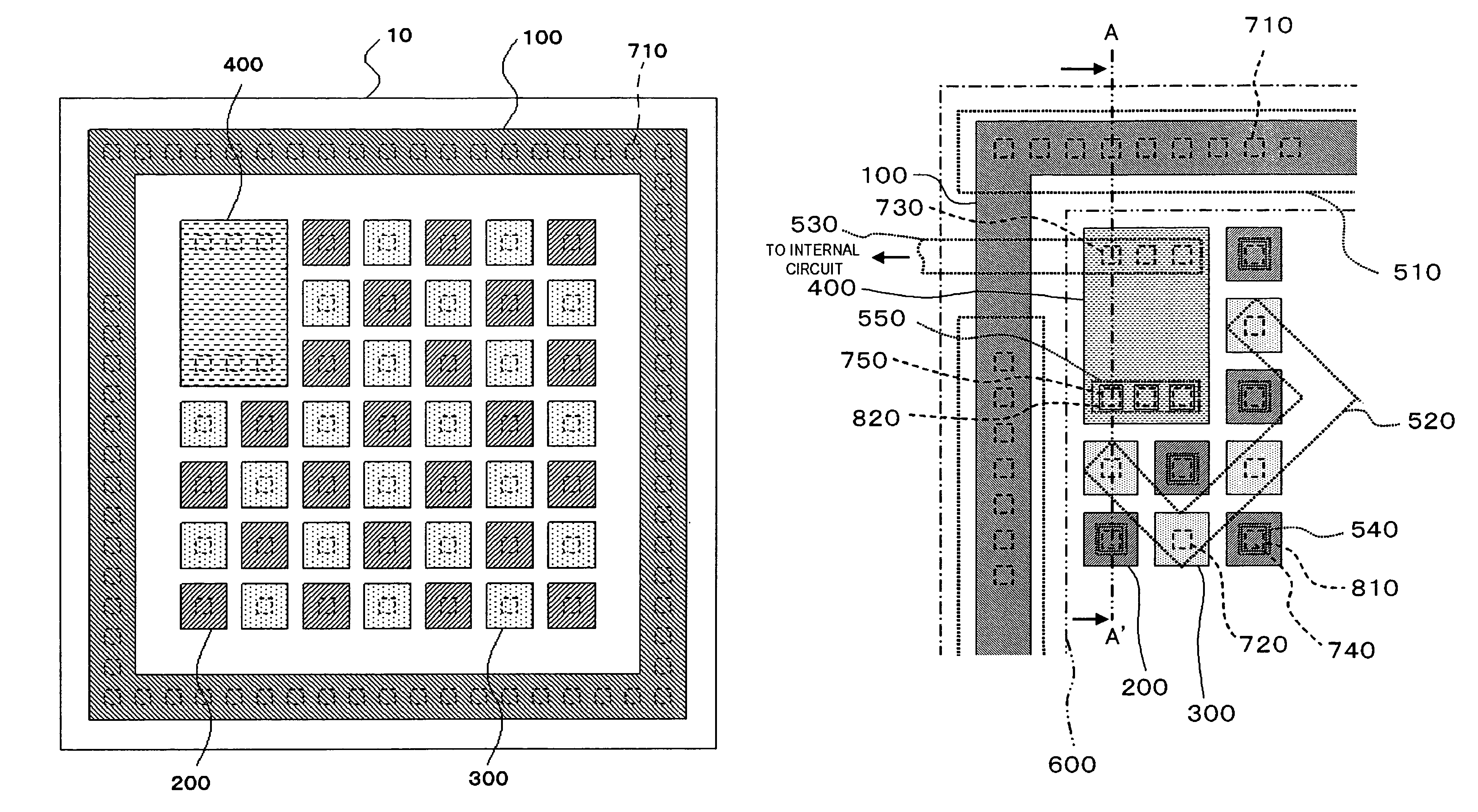
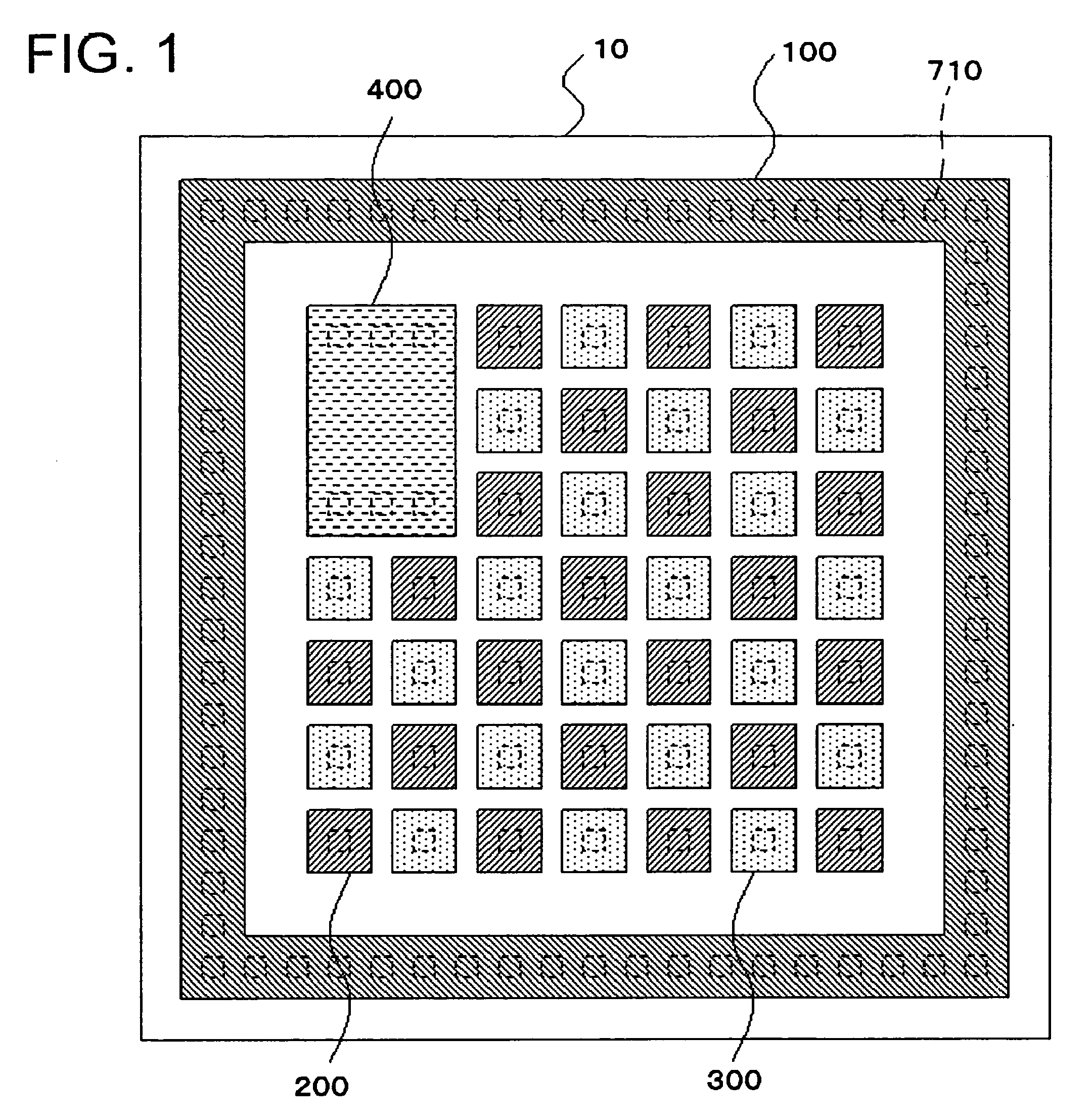
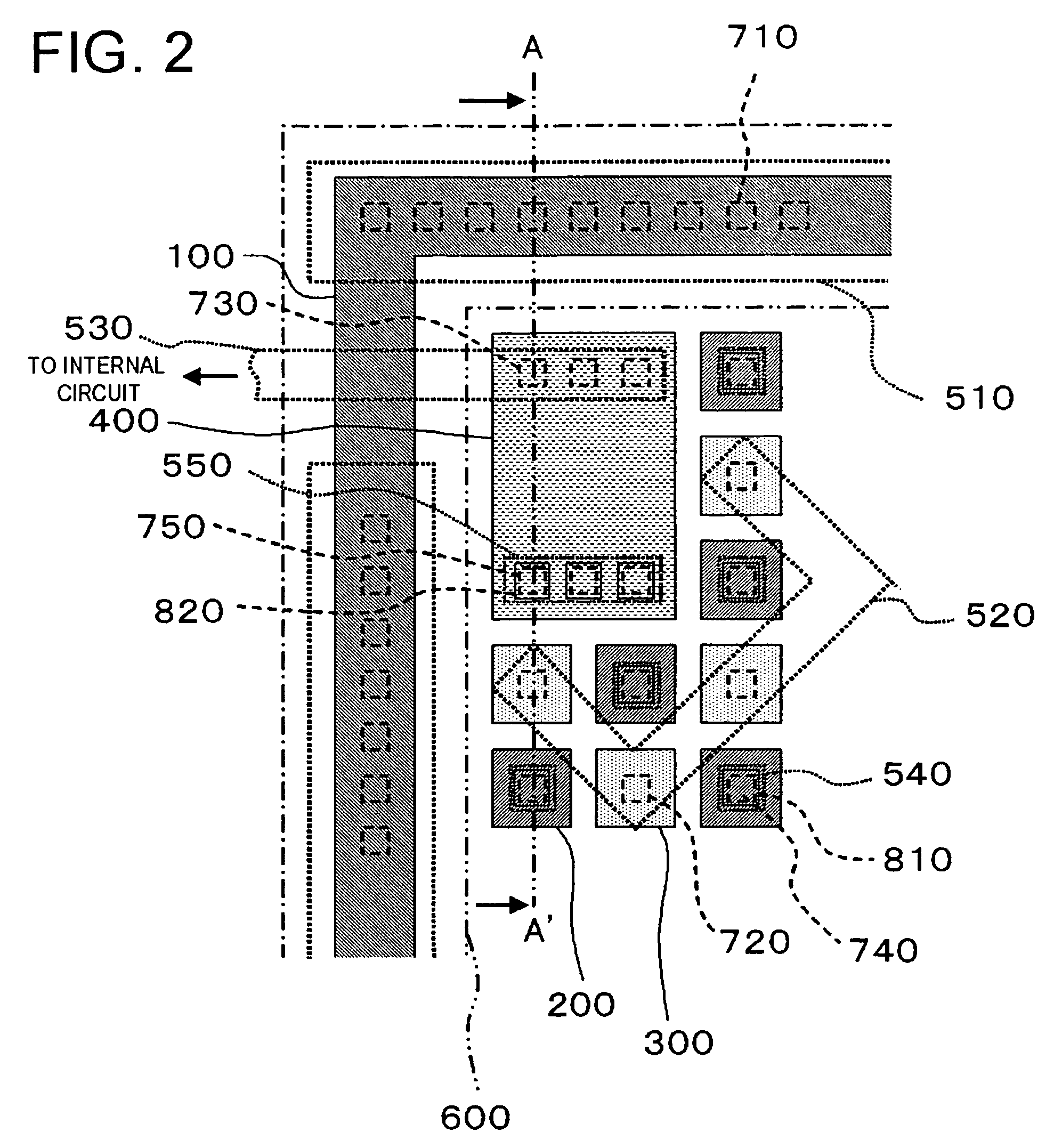
[0026]FIG. 1 is a plan view explaining a configuration of a semiconductor device of the first embodiment. The semiconductor device has a protective element. The protective element has a first-conductivity-type well 10, a plurality of first diffusion layers 200 formed in the well 10, a plurality of second diffusion layers 300 formed in the well 10, and a diffusion resistance layer 400 formed in the we...


PUM


Abstract

Aimed at reducing the area of a protective circuit in a semiconductor device provided therewith, a semiconductor device of the present invention has a first-conductivity-type well, a plurality of first diffusion layers formed in the well, a plurality of second diffusion layers formed in the well, and a diffusion resistance layer formed in the well, wherein the first diffusion layers have a second conductivity type, and are connected in parallel with each other to an input / output terminal of the semiconductor device; the second diffusion layers are arranged alternately with a plurality of first diffusion layers, and are connected to a power source or to the ground; the diffusion resistance layer has a second conductivity type, and is located in adjacent to any of the plurality of second diffusion layers; the diffusion resistance layer is connected to the input / output terminal of the semiconductor device, while being arranged in parallel with the first diffusion layers, and connects the internal circuit and the input / output terminal of the semiconductor device.

Description

[0001]This application is based on Japanese patent application No. 2008-083700 the content of which is incorporated hereinto by reference.BACKGROUND[0002]1. Technical Field[0003]The present invention relates to semiconductor a device having a protective element.[0004]2. Related Art[0005]For the case where a protective element for protecting an internal circuit from static electricity or the like is provided to a semiconductor device, it is most general to arrange a resistive element for limiting current between the protective element and the internal circuit, to thereby prevent over-current from flowing into the internal circuit. The resistive element is typically a polysilicon resistor composed of polysilicon, or a diffusion layer resistor composed of a diffusion layer. In some cases where the diffusion layer resistor is used, it may be integrated with the protective element so as to reduce the occupied area (see Japanese Laid-Open Patent Publication Nos. 02-070229 and 06-302765, f...

Claims


Application Information

Patent Timeline
Patent Type & Authority Patents(United States)
IPC IPC(8): H01L29/66
CPCH01L27/0259
Inventor NAGAI, TAKAYUKI
Owner RENESAS ELECTRONICS CORP
Why Eureka
Try Eureka