Measurement of pixel current in display device

a display device and current measurement technology, applied in the field of display devices, can solve the problems of comparatively long time taken to measure one pixel current, inconsistencies in brightness, and difficulty in measuring current of a particular specified pixel by measuring power supply current of the panel, so as to speed up the rise time of pixel current flowing and eliminate pixel current. , the effect of accurate pixel current measuremen

Active Publication Date: 2011-12-06
GLOBAL OLED TECH
View PDF7 Cites 6 Cited by
  • Summary
  • Abstract
  • Description
  • Claims
  • Application Information

AI Technical Summary

Benefits of technology

[0020]According to the present invention, PVDD lines other than horizontal line to which a pixel being measured belongs are isolated, which shows that it is possible to eliminate pixel current that includes leakage current when the other lines are unlit, and parasitic capacitance of the PVDD line (capacitive component of the distributed constant circuit 3 shown in FIG. 5) is reduced, speeding up the rise time of pixel current flowing to the power supply. Also, according to this method, it is possible to perform measurement of pixel current while carrying out normal image display. This shows that it is possible to measure pixel current during image display and correct brightness irregularities. It is also possible to perform accurate pixel current measurement from comparison at the time of illumination and non-illumination.

Problems solved by technology

If there are variations in Vth and μ of the TFT inside the panel, there will usually be inconsistencies in brightness.
1) According to the prior art, image current is measured in real time during image display. In order to suppress effects of aging of the drive TFTs and organic EL elements, it is necessary to measure the current of each particular specified pixel independently. However, during image display, current corresponding to a display image constantly flows in from a power supply, which shows that it is difficult to measure current of a particular specified pixel by measuring power supply current of the panel.
2) FIG. 1 is one example of a pixel circuit, but in actual fact, as shown in FIG. 5, there are distributed constant circuits on each power supply line and signal line due to wiring resistance and stray capacitance etc. Specifically, there are RC distributed constant circuits in the data lines Data between the source driver 10 and the drain of the select TFT 2, in the gate lines Gate between the gate driver 12 and the gate of the select TFT 2, in the power supply lines between the power supply PVDD and the source of the drive TFT 1, and between the cathodes of the organic EL element 3 and the power supply CV.
Accordingly, it is necessary to perform measurement of current with current at a sufficient level of stability, but the fastest measurement time is determined by this, and a comparatively long time is taken to measure one pixel current.
In particular, in the event that leakage current varies over time, it constitutes a noise component, which shows that measurement accuracy will be affected.

Method used


Image

  • Measurement of pixel current in display device
  • Measurement of pixel current in display device
  • Measurement of pixel current in display device

Examples


Embodiment Construction

[0037]Embodiments of the present invention will be described in the following based on the drawings.

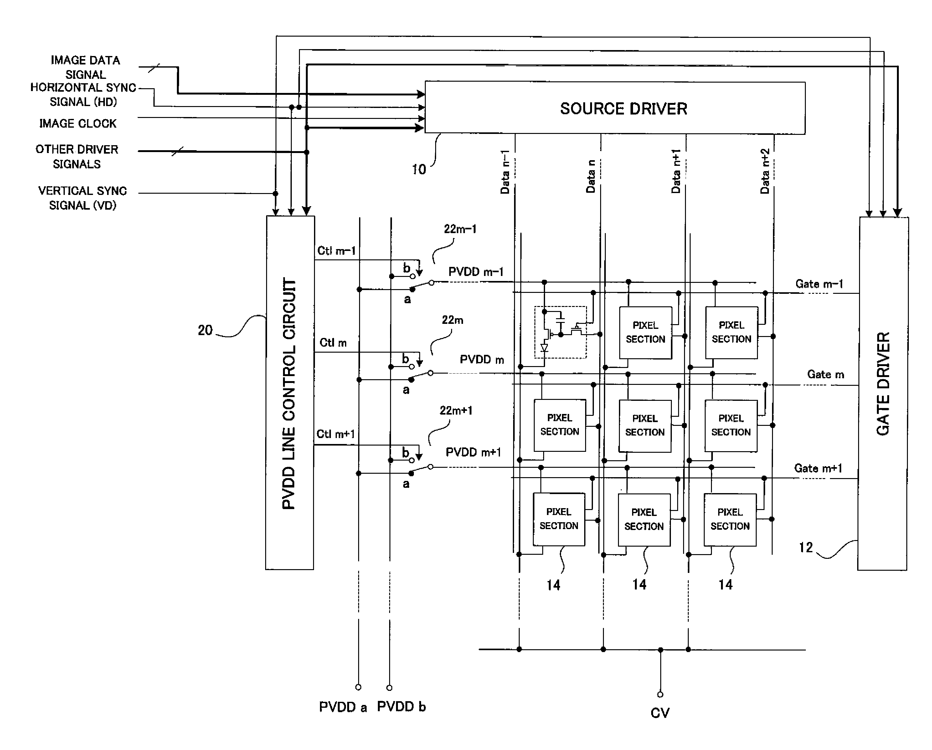
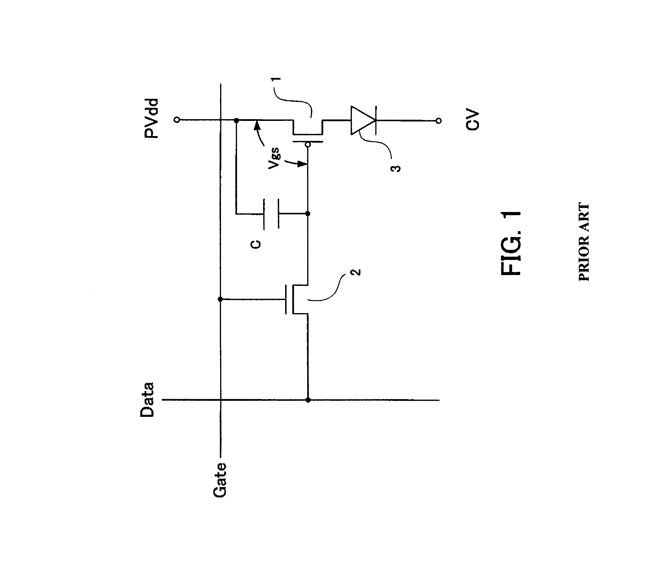
[0038]As shown in FIG. 6, this embodiment also has a source driver 10, a gate driver 12, and a pixel section 14 arranged in a matrix shape. Also, gate lines Gate extends from the gate driver 12 to each row. With this example, a P-channel transistor has been used as the select TFT 2, and is turned on when Gate is at an L level.

[0039]This embodiment has a PVDD line control circuit 20. A horizontal sync signal (HD), a vertical sync signal (VD) and other drive signals are supplied to this PVDD line control circuit. Horizontal PVDD lines are also provided along each pixel line, and each horizontal PVDD line is switchably connected to a vertical PVDDa line or a vertical PVDDb line by respective switches 22. The vertical PVDDa lines and vertical PVDDb lines are connected to respectively separate power supplies PVDDa and PVDDb. In FIG. 6, three horizontal PVDD lines, PVDDm−1, PVDDm and PVDDm+...


PUM


Abstract

During image display, pixel current measurement for brightness irregularity correction is carried out. Display is carried out by sequentially writing pixel data in a horizontal direction to pixel sections that are arranged in a matrix shape. Horizontal power supply lines PVDD are arranged for each horizontal line, and power is supplied from these power supply lines to corresponding pixel sections. When carrying out measurement of pixel current by lighting pixel sections one at a time, a horizontal power supply line PVDD of a horizontal line to which the lit pixel belongs is connected to a power supply PVDDb by a switch, and other horizontal power supply lines PVDD are connected to PVDDa.

Description

CROSS-REFERENCE TO RELATED APPLICATION[0001]This application claims priority of Japanese Patent Application No. 2007-330797 filed Dec. 21, 2007 which is incorporated herein by reference in its entirety.FIELD OF THE INVENTION[0002]The present invention relates to a display device for writing pixel data for each pixel arranged in a matrix shape, and performing display.BACKGROUND OF THE INVENTION[0003]FIG. 1 shows the structure of a circuit for one pixel section (pixel circuit) of a basic active organic EL display device, and FIG. 2 shows the structure, and input signals of, a display panel.[0004]A data signal is written to a storage capacitor C by setting a gate line (Gate) that extends in the horizontal direction to a high level to turn an n-channel selection TFT 2 on, and in this state placing a data signal (image data) having a voltage corresponding to a display brightness on a data line (Data) that extends in the vertical direction. In this way, a gate of a p-channel drive TFT 1 i...

Claims


Application Information

Patent Timeline
Patent Type & Authority Patents(United States)
IPC IPC(8): G09G3/30
CPCG09G3/3233G09G2300/0842G09G2300/0866G09G2320/0285G09G2320/0295G09G2320/043G09G2320/0693
Inventor MIZUKOSHI, SEIICHIKOHNO, MAKOTOONOMURA, KOUICHIKAWABE, KAZUYOSHI
Owner GLOBAL OLED TECH
Why Eureka
Try Eureka